Fall 2023 - Chemical Engineering 4420 "Fabricating a Semiconductor Diode"
Week 1 - Dr. Sergi Lendinez discusses the fundamentals of the fabrication process and reviews the tools students will use to fabricate their devices
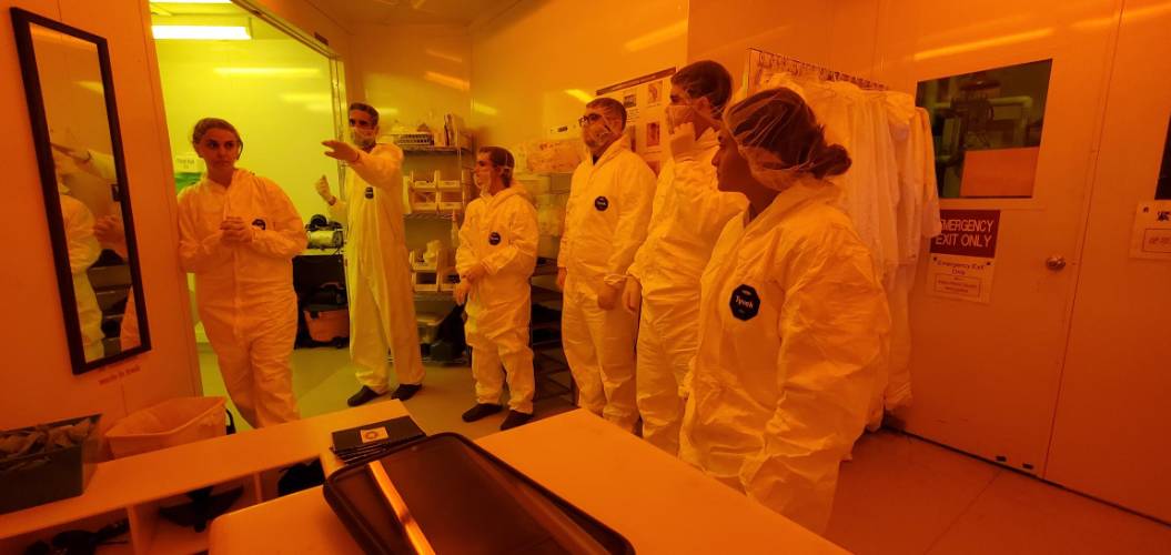
Image 1 - Class Orientation
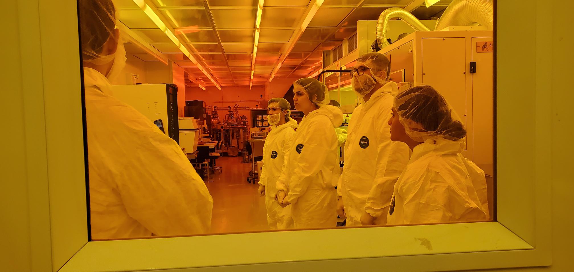
image 2 - Cleanroom Tour
Week 2 - LSU Chemical Engineering Professor/NFF Director, Dr. Kevin McPeak introduced students to the basics of thin film thickness measurement and how Ellipsometry is used to characterize films

Image 1 - Woollam RC2
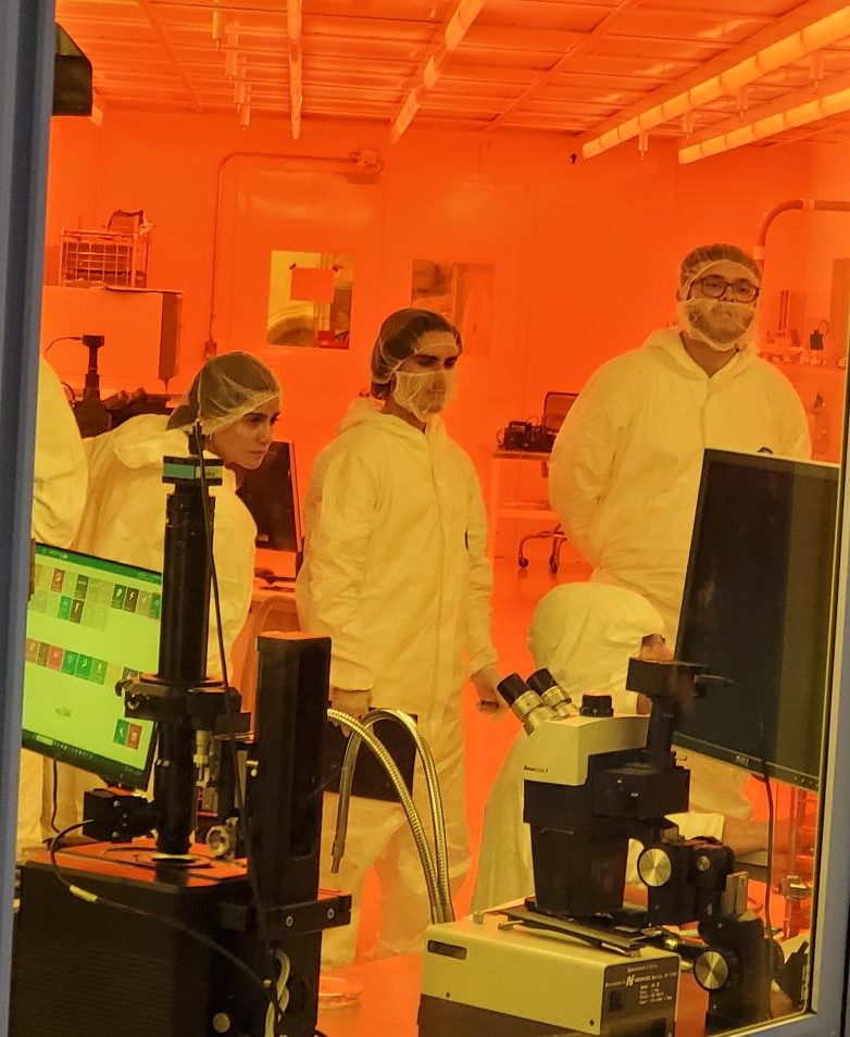
Image 2 - Data collection
Week 3 - Students began prepping samples for resist coating followed by review of the Quantum ML3Pro which students will use to align and expose their samples
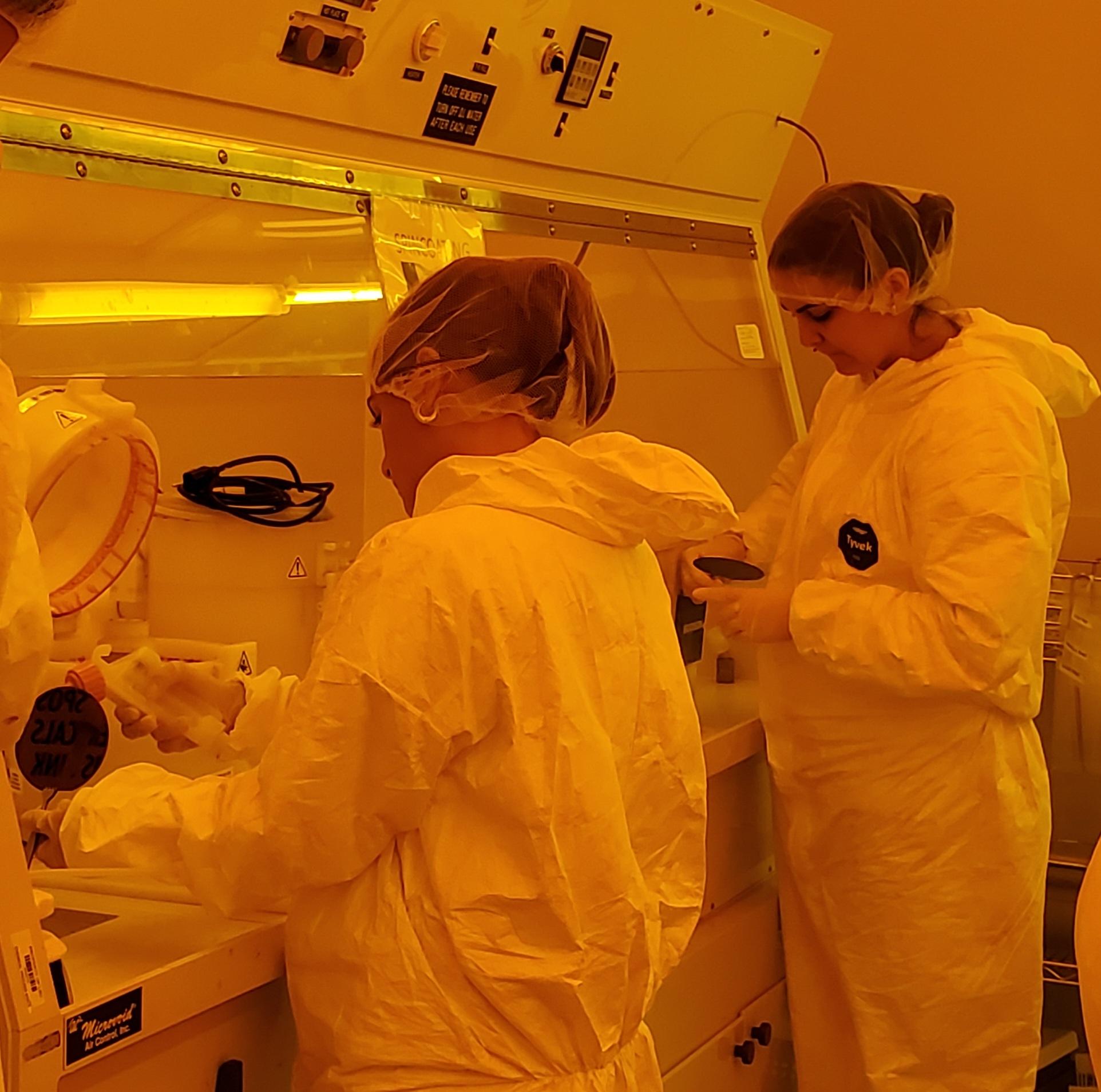
Image 1 - Sample cleaning
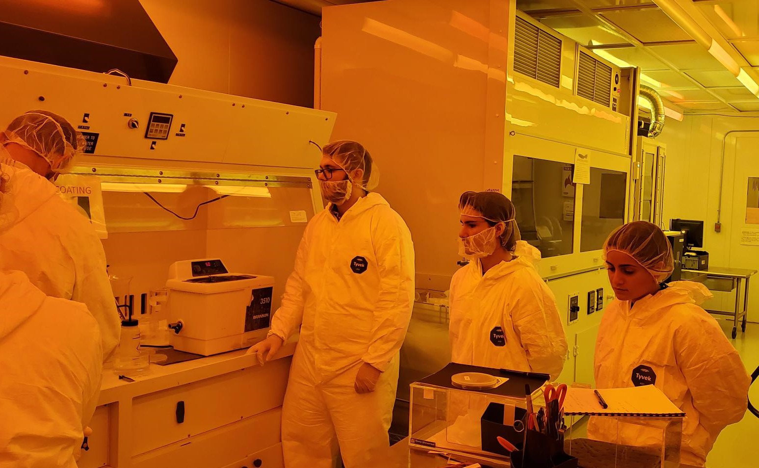
Image 2 - Resist Application
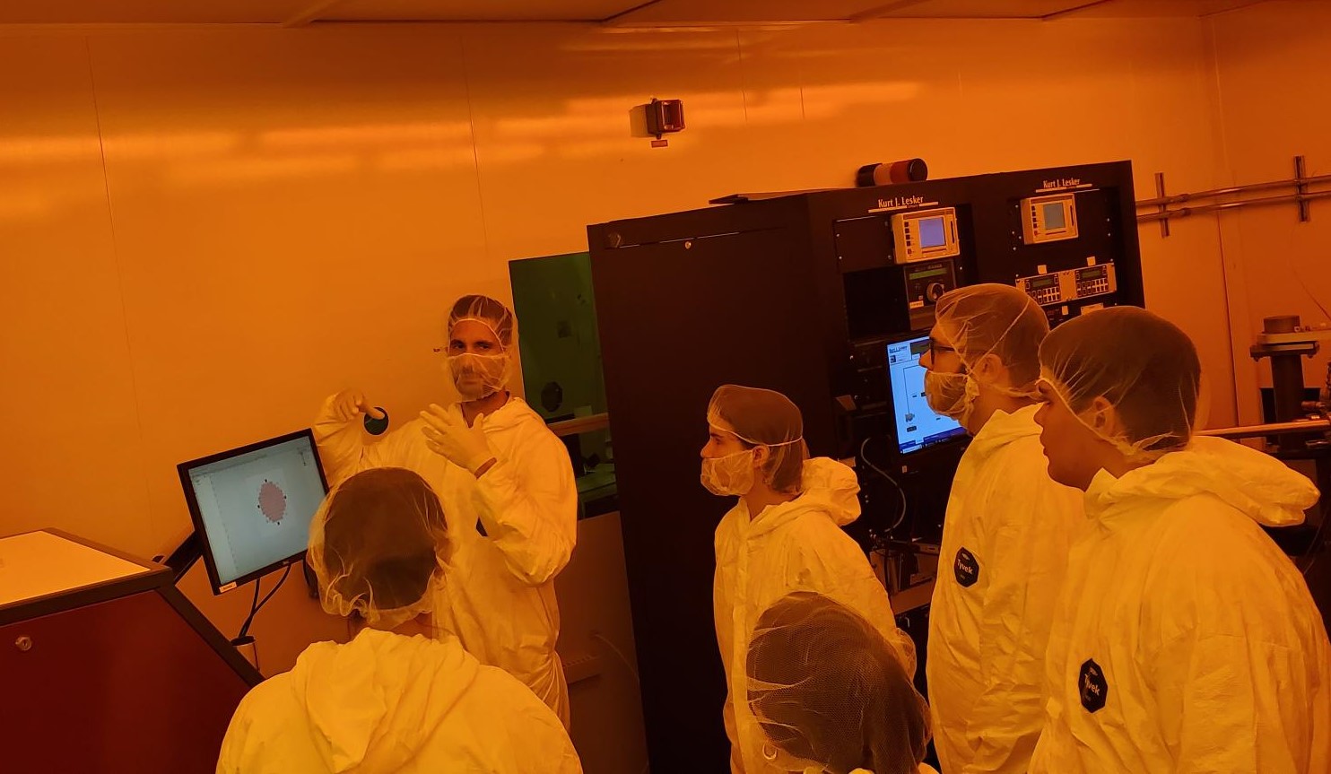
Image 3 - UV Exposure
Week 4 - SiO2 layer etched using Oxford Instruments DRIE/ICP followed by resist stripping, Spin On Dopant layer and exposure.
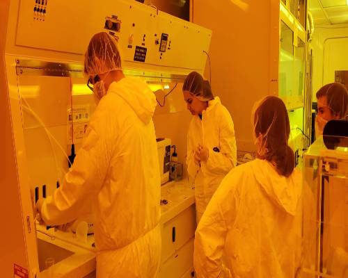
Image 1 - Resist stripping/RCA Cleaning
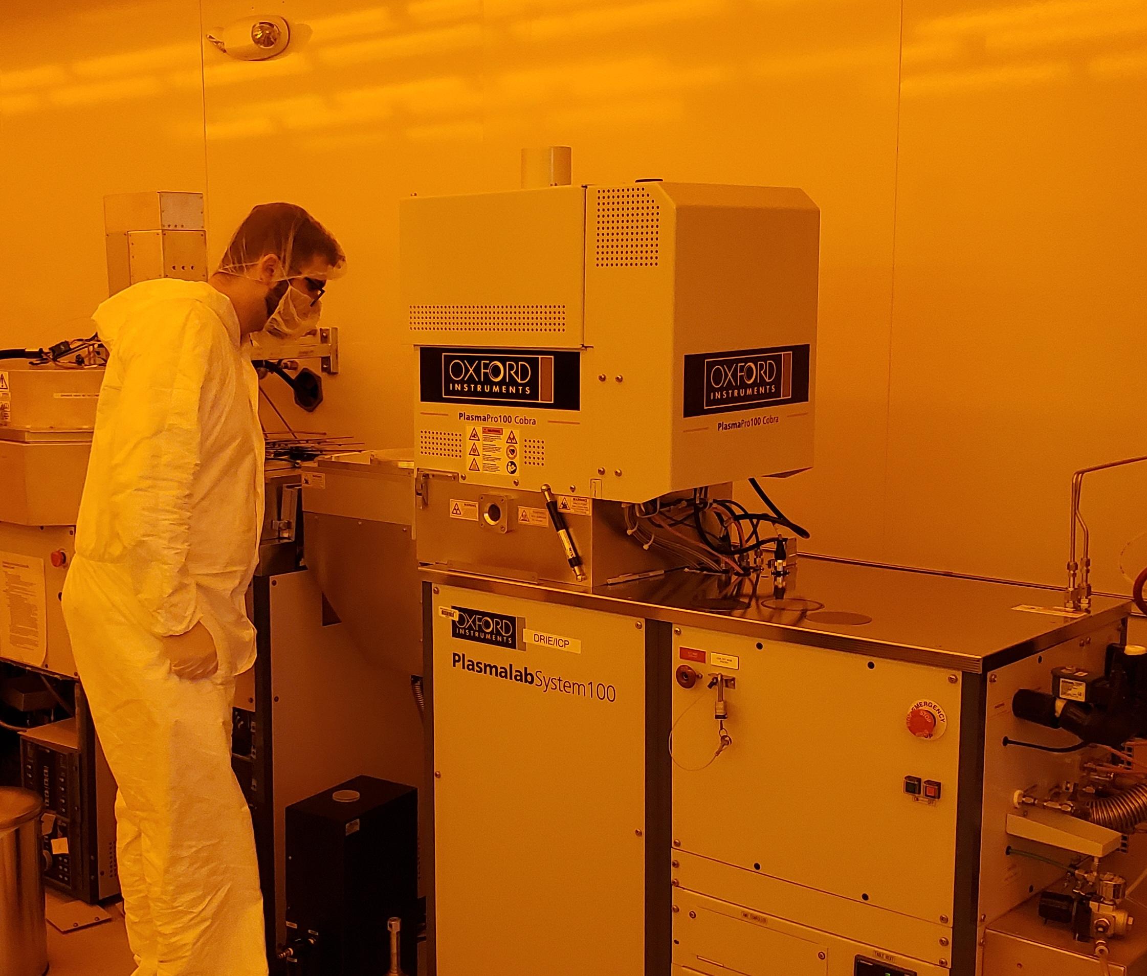
Image 2 - Oxide layer removal
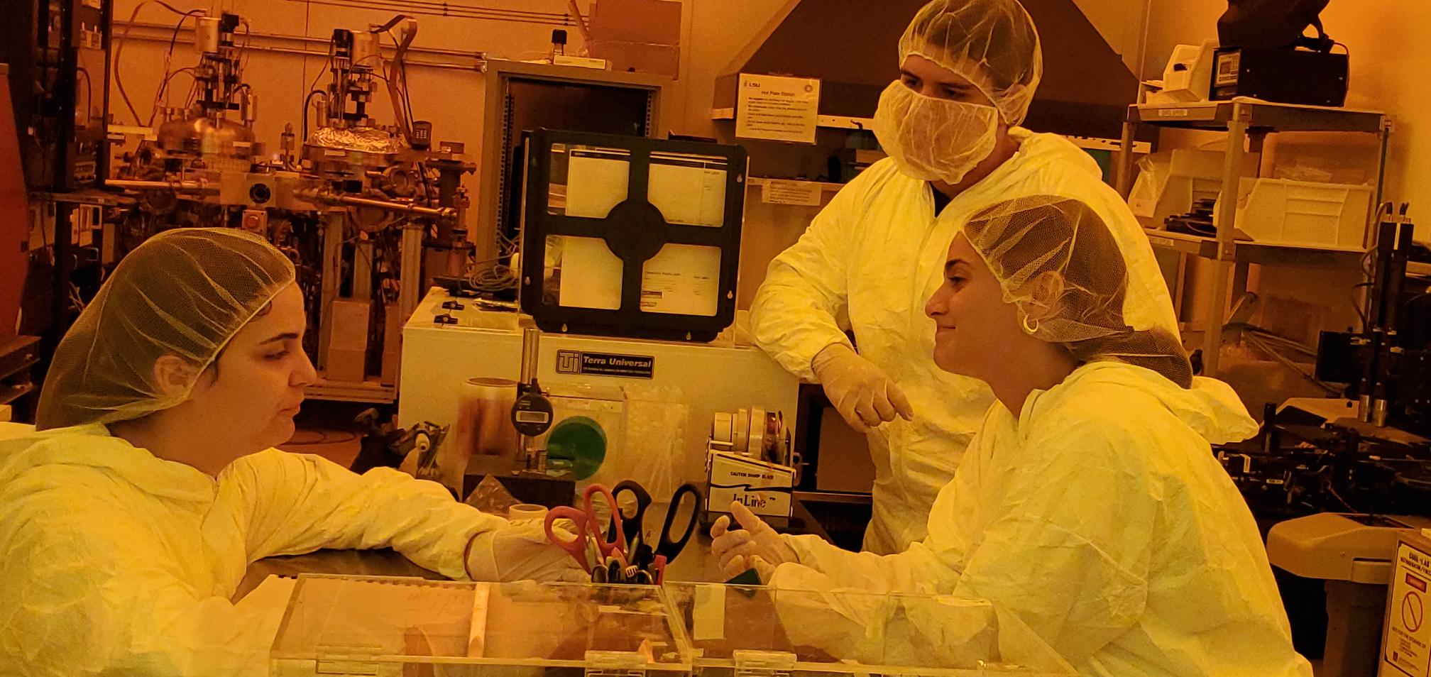
Image 4 - Students review first layer application steps
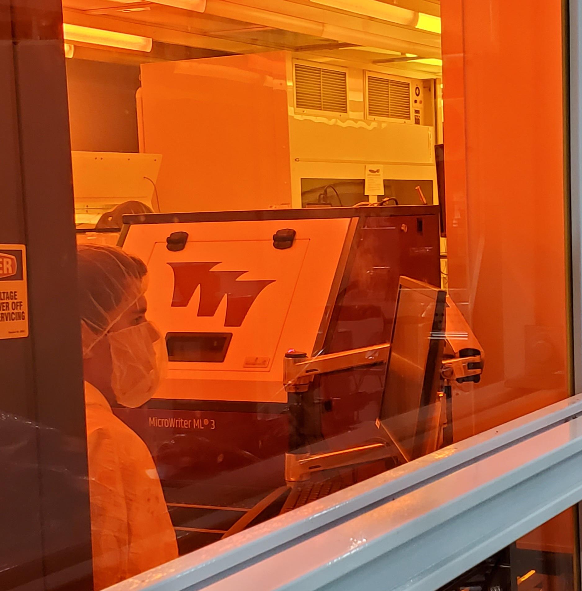
Image 3 - First layer exposure
Week 5 - Students finished processing the first layer of their samples. Dopant layer removed from last week's application followed by microscopic inspection
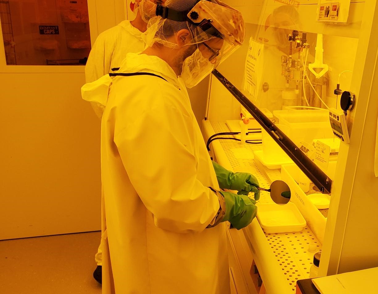
Image 1 - HF (SOD Removal)
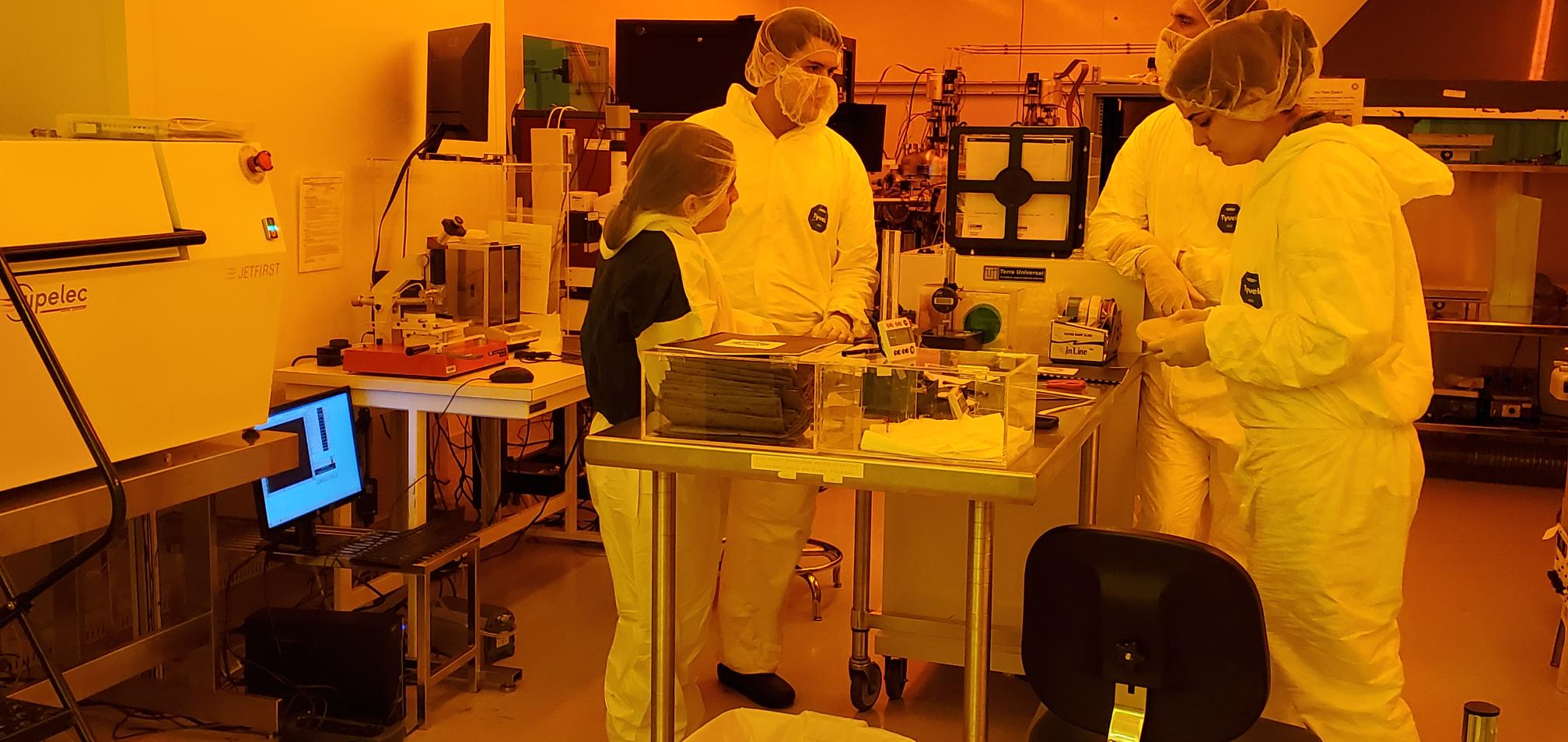
Image 3 - Class review of "Spin on Dopant" etch process
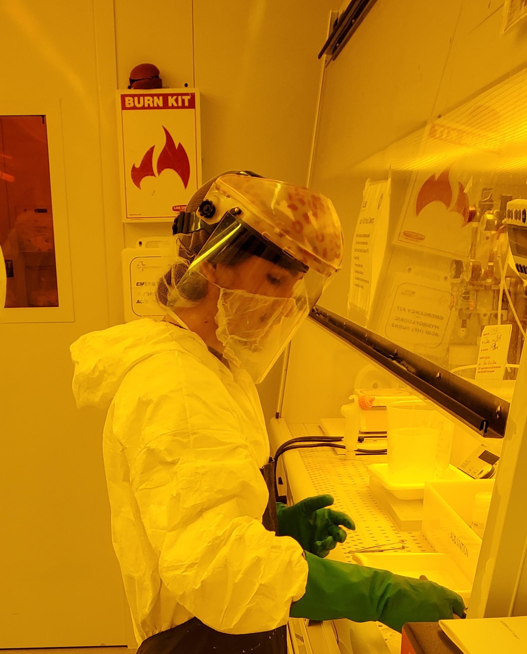
Image 2 - Etch solution prep
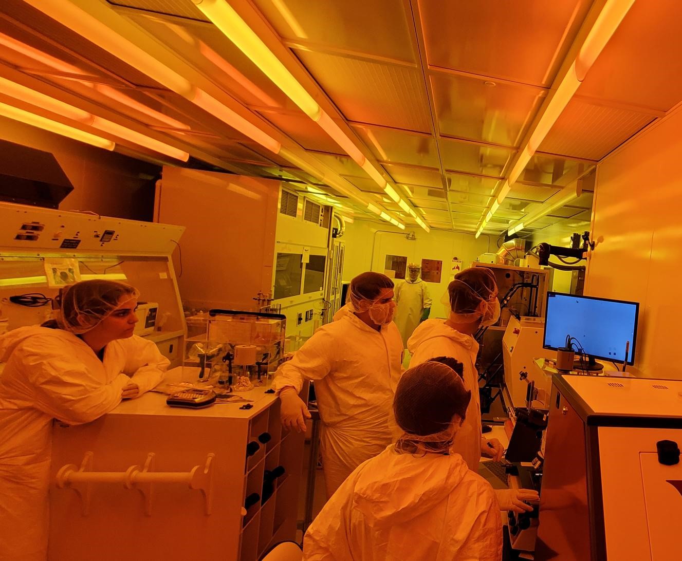
Image 4 - Microscopic Inspection
Week 6 - Students prepped samples for the second layer application
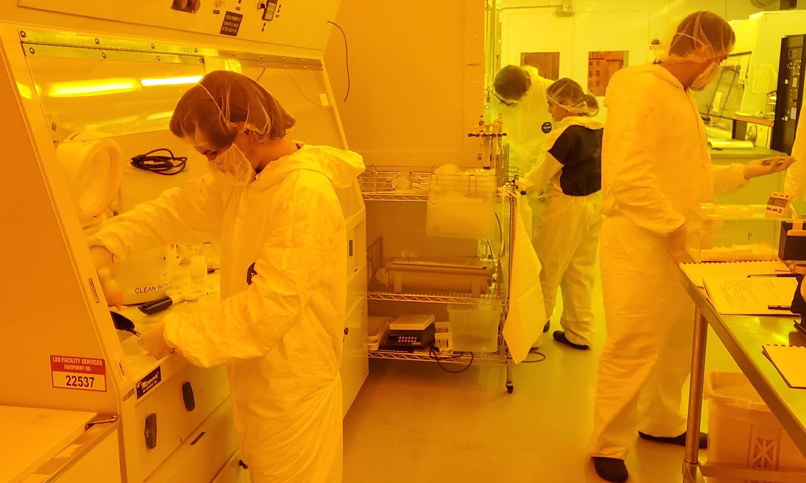
Image 1 - Sample cleaning
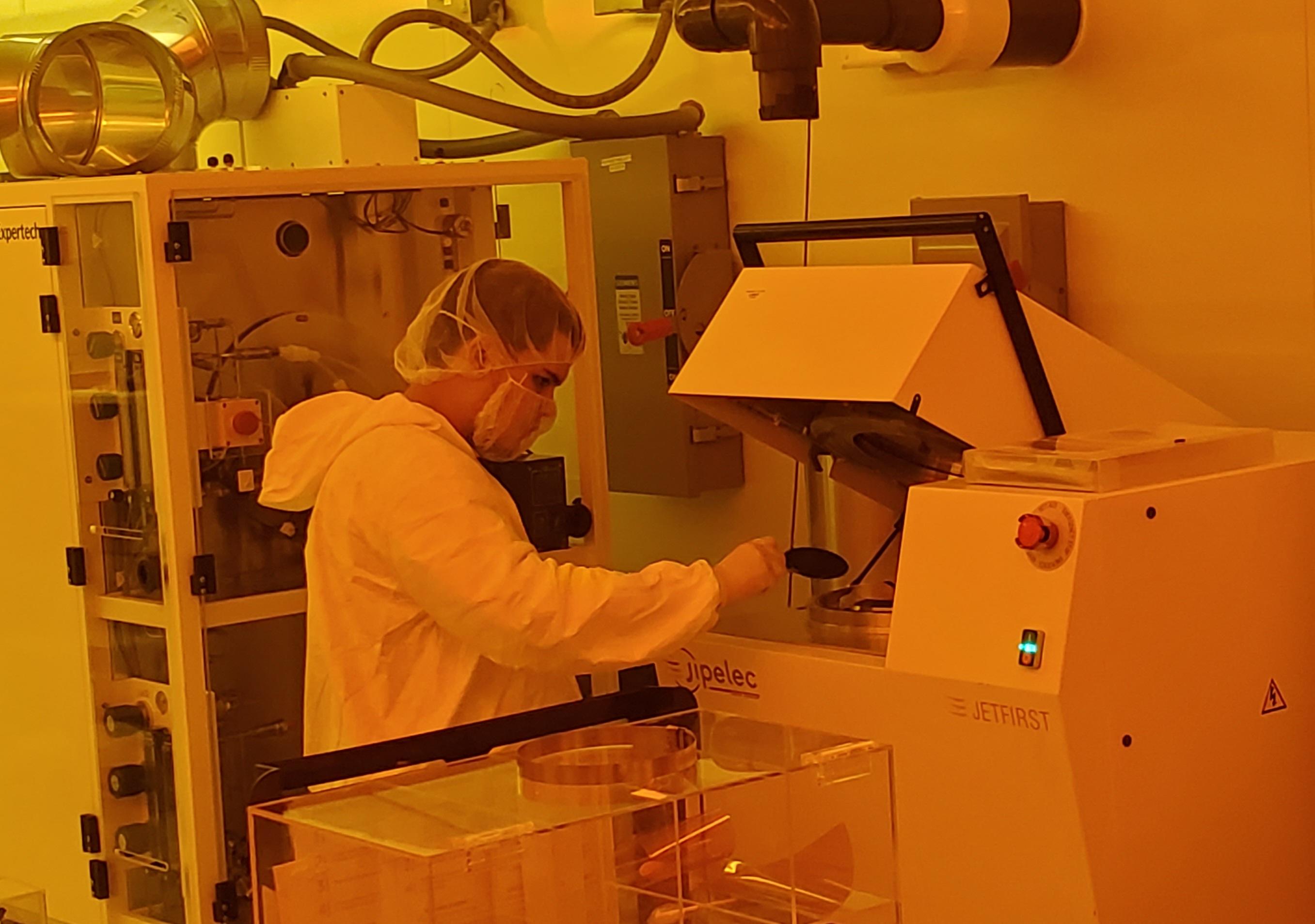
Image 2 - RTA ( Rapid Thermal Annealing)
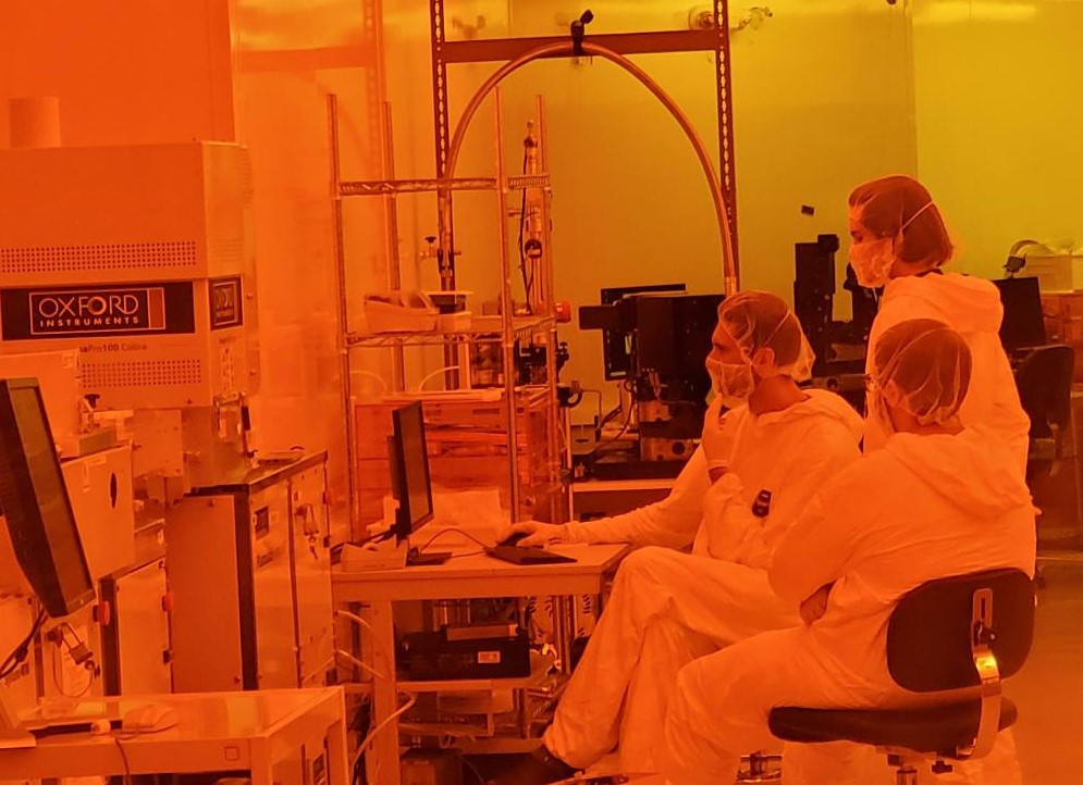
Image 3 - DRIE/ICP Etch
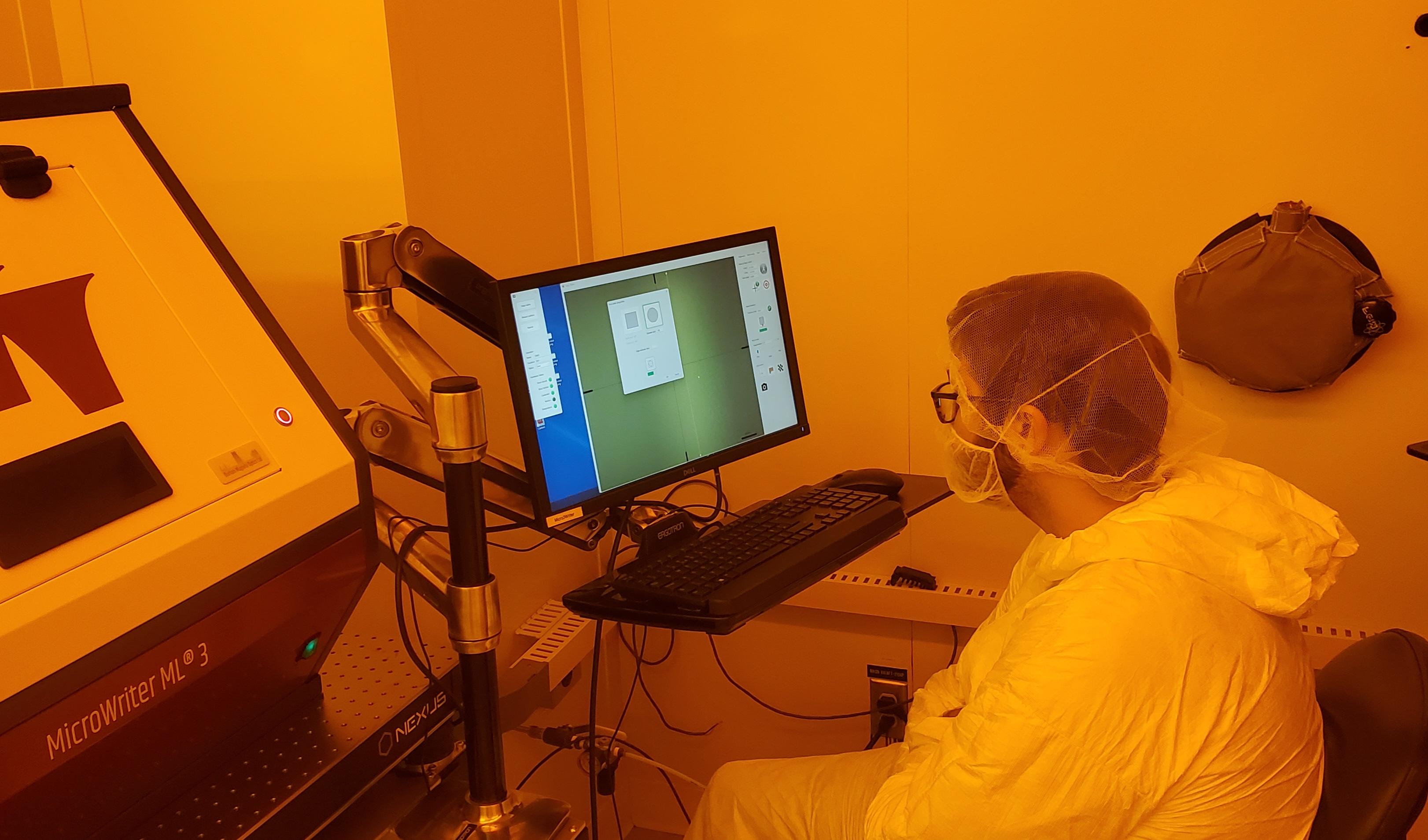
Image 4 - Alignment inspection
Week 7 - Students completed the second layer application. Spincoating followed by a soft bake, second layer exposure and development
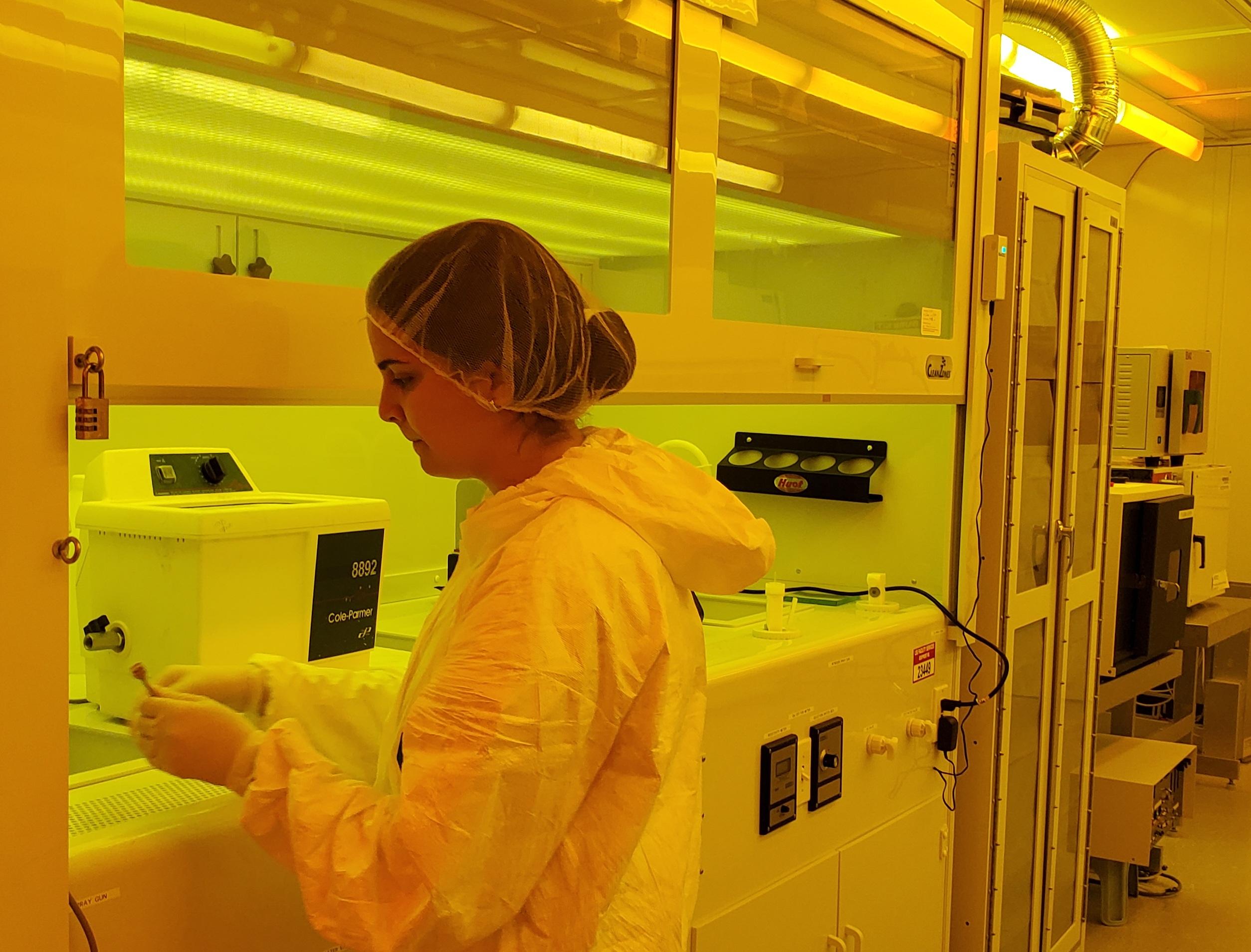
Image 1 - Sample Development
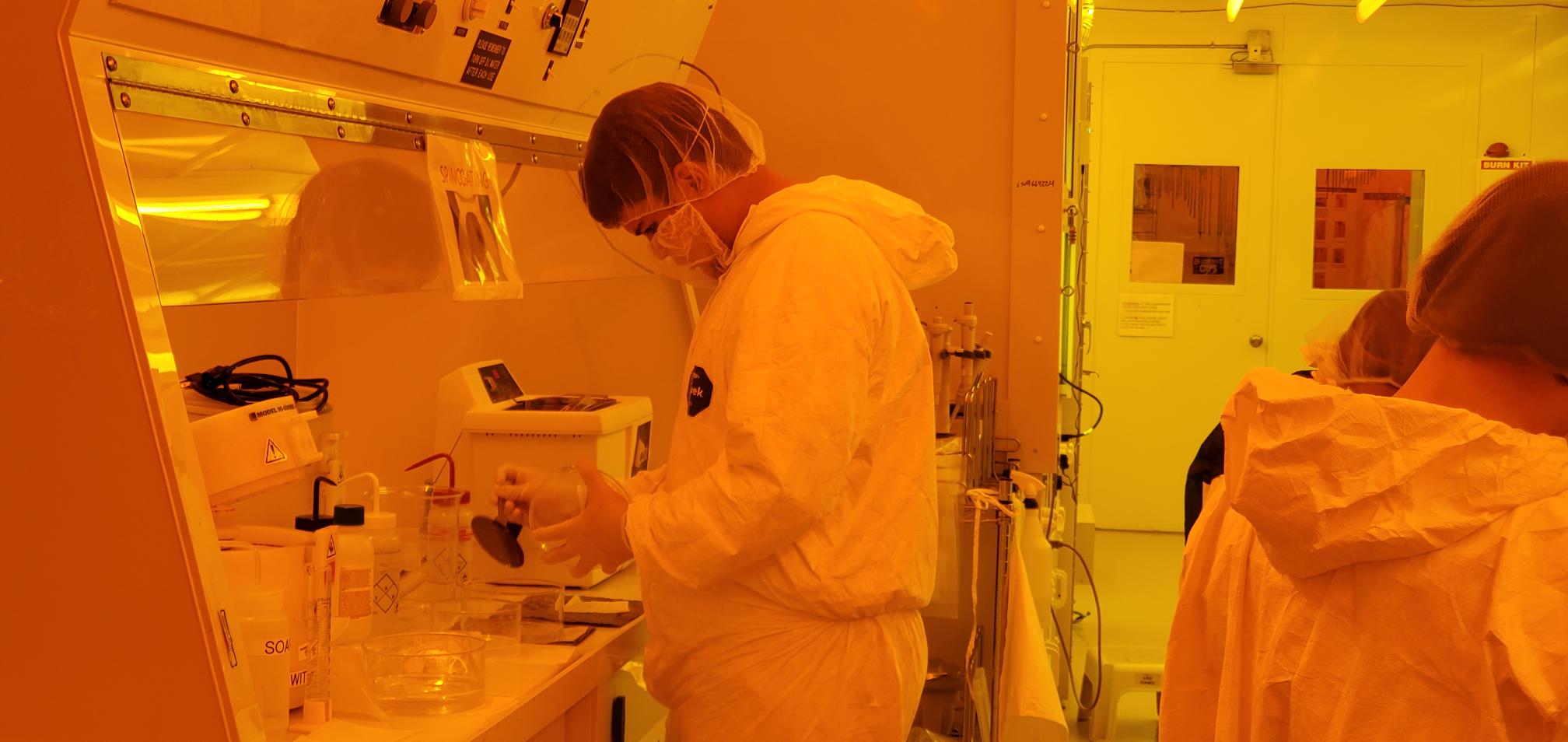
Image 2 - Sample Cleaning
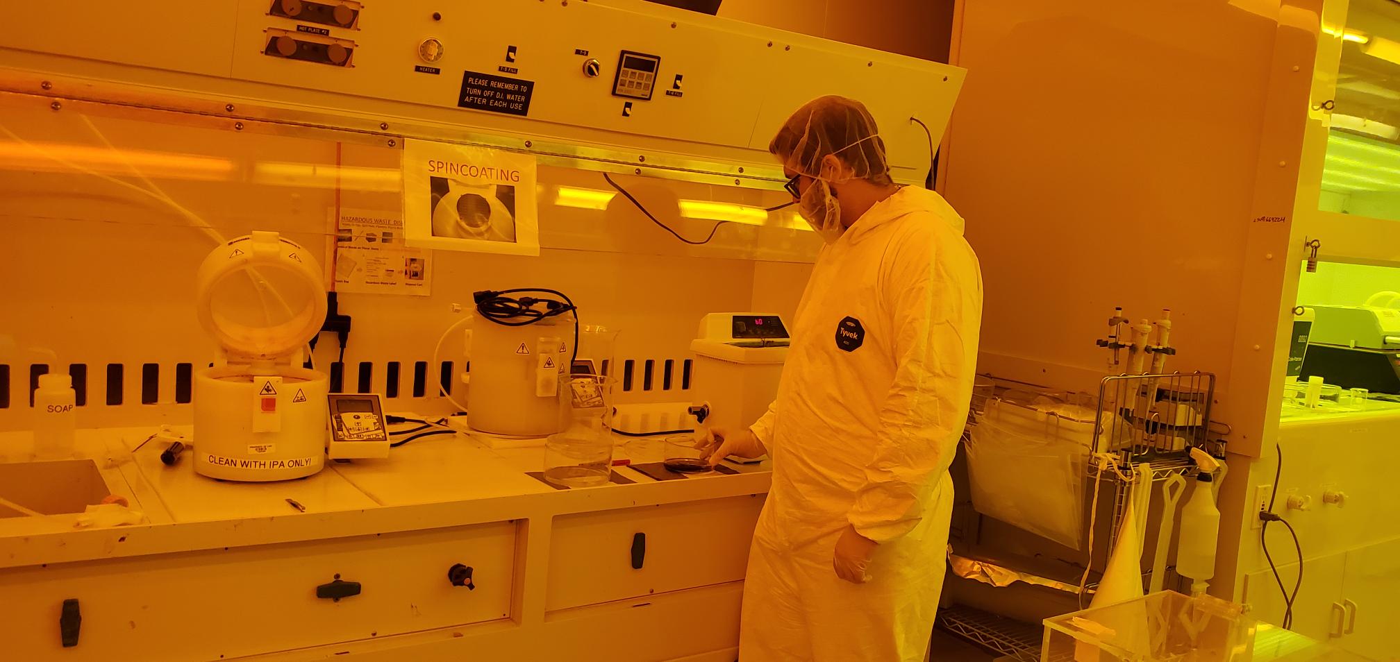
Image 3 - Etching
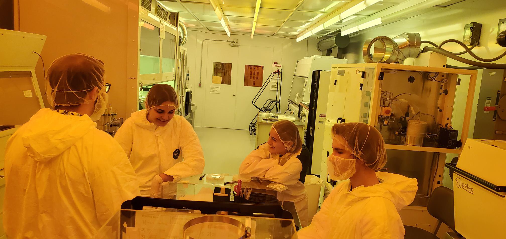
Image 4 - "Layer 3" application discussions
Week 8 - Students applied the final layer to their samples followed by metal layer deposition
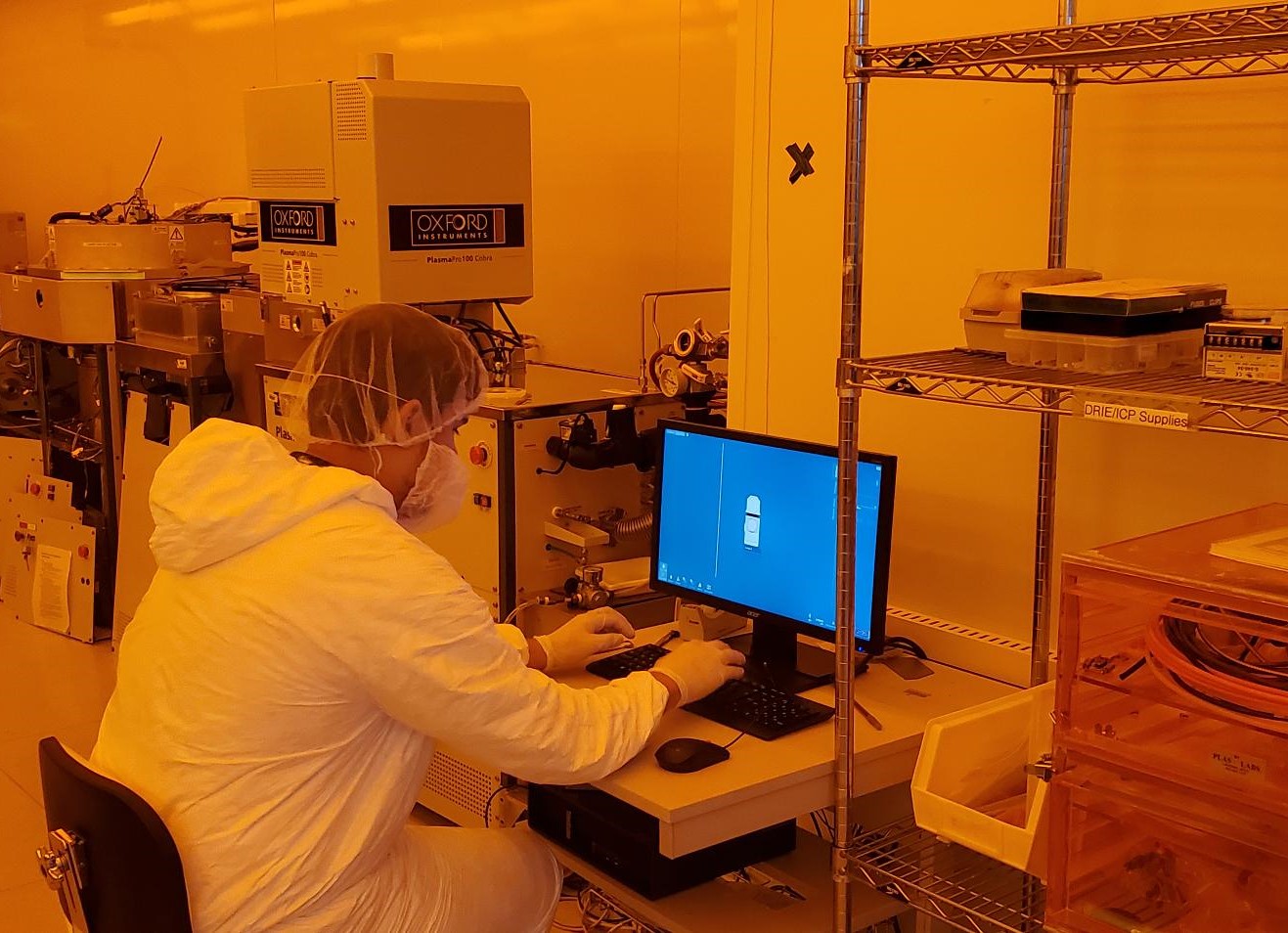
Image 1 - Third Layer Etch
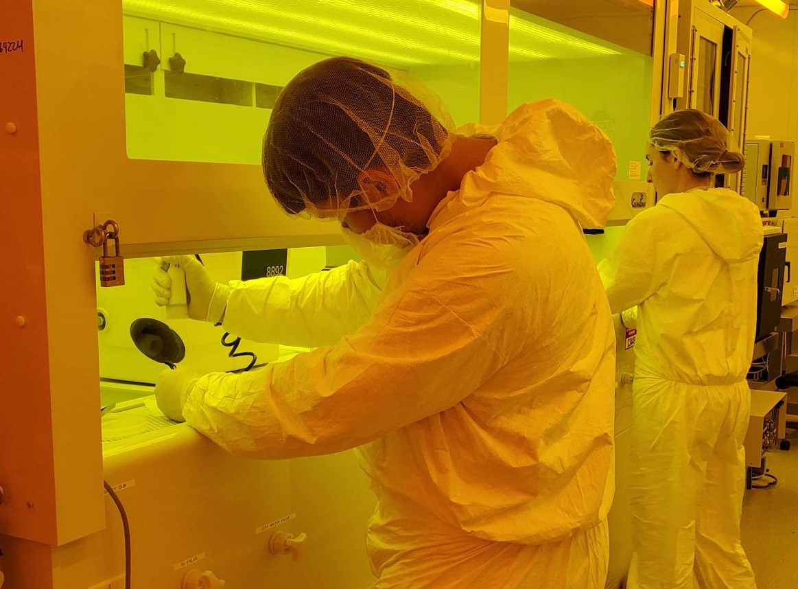
Image 2 - Sample Development
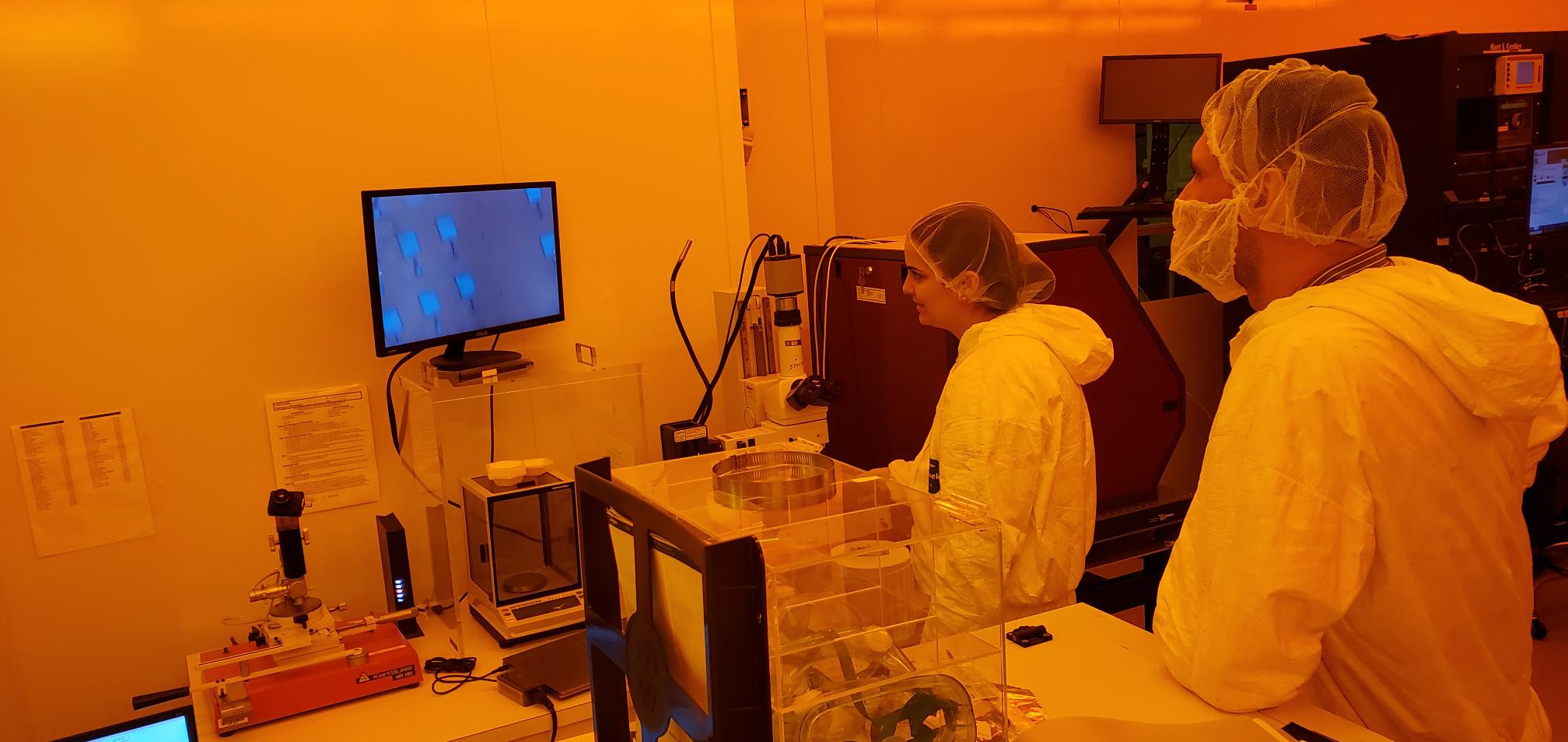
Image 3 - Microscopic Verification
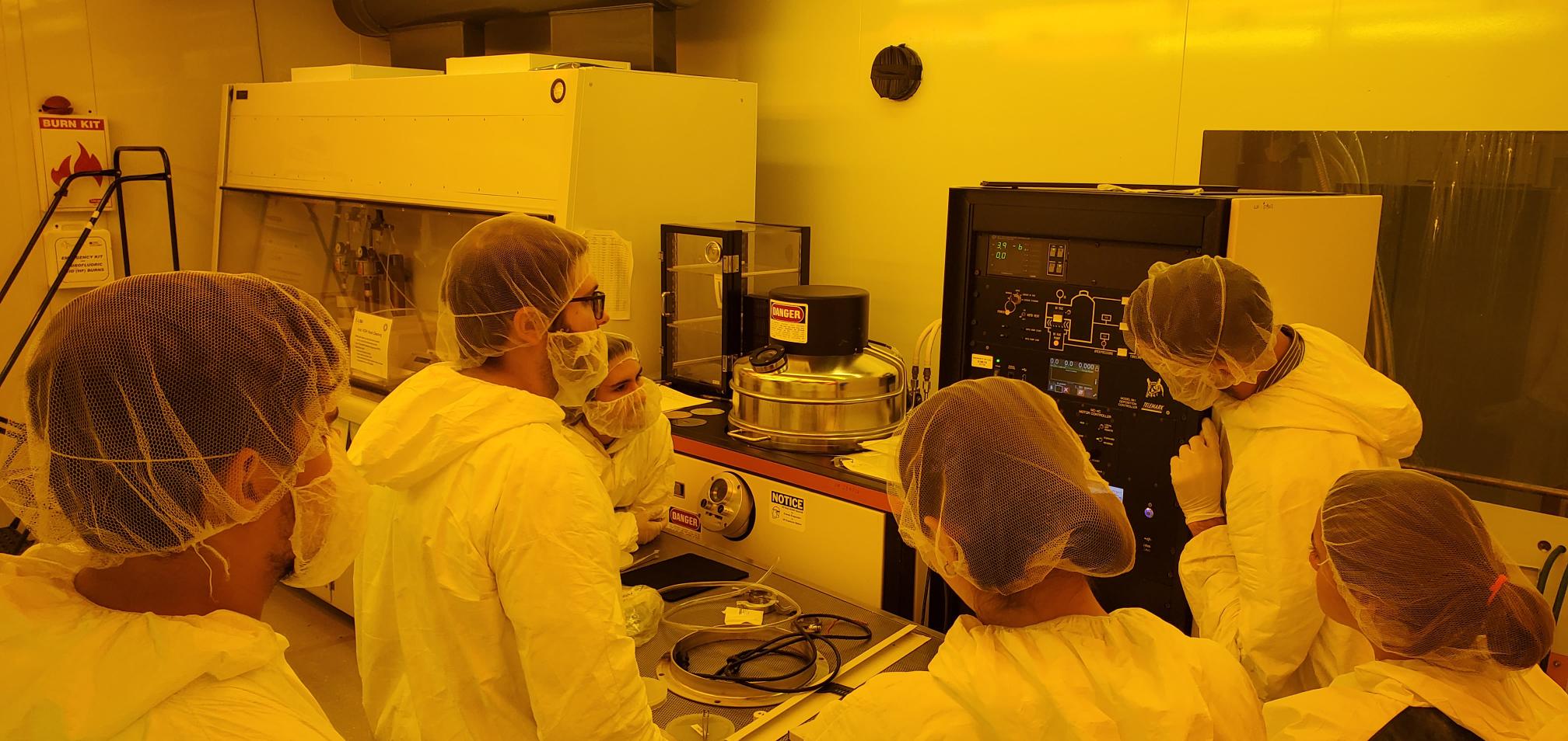
Image 4 - Ebeam Deposition Overview
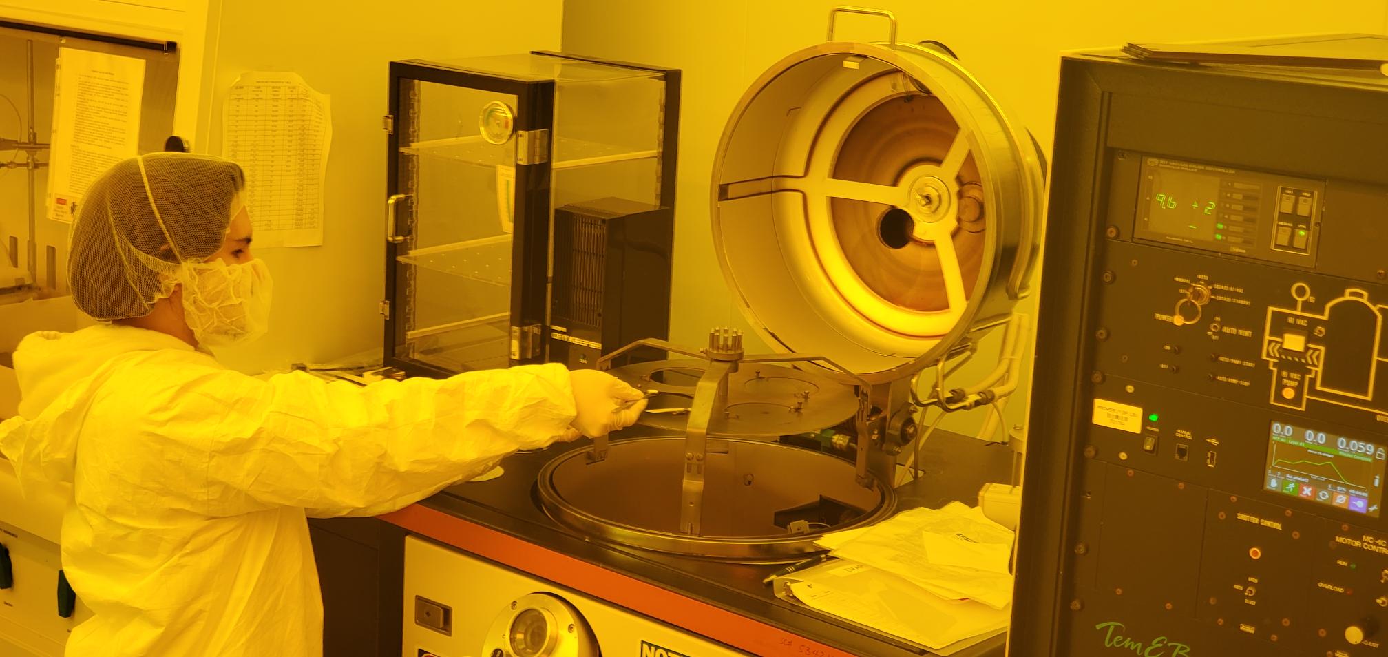
Image 5 - Metal Layer Deposition
Week 9 -.Students tested their samples for an electrical current then measured the electrical properties by AFM
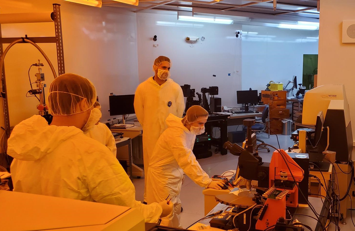
Image 1 - Probe Station Sample Set Up
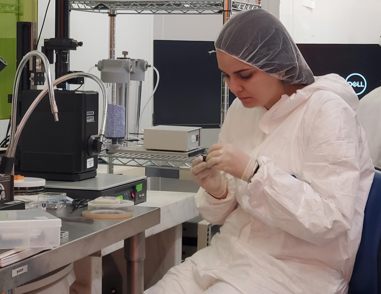
Image 4 - AFM Tip Change
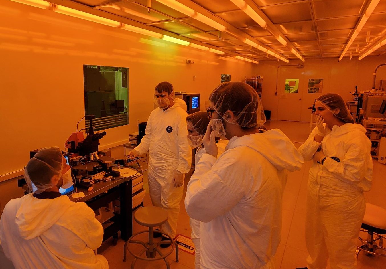
Image 2 - Probe Station Class Review
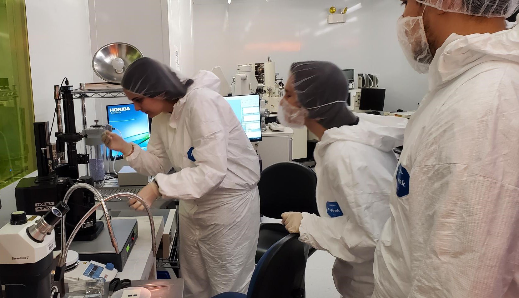
Image 5 - AFM Sample Set-Up
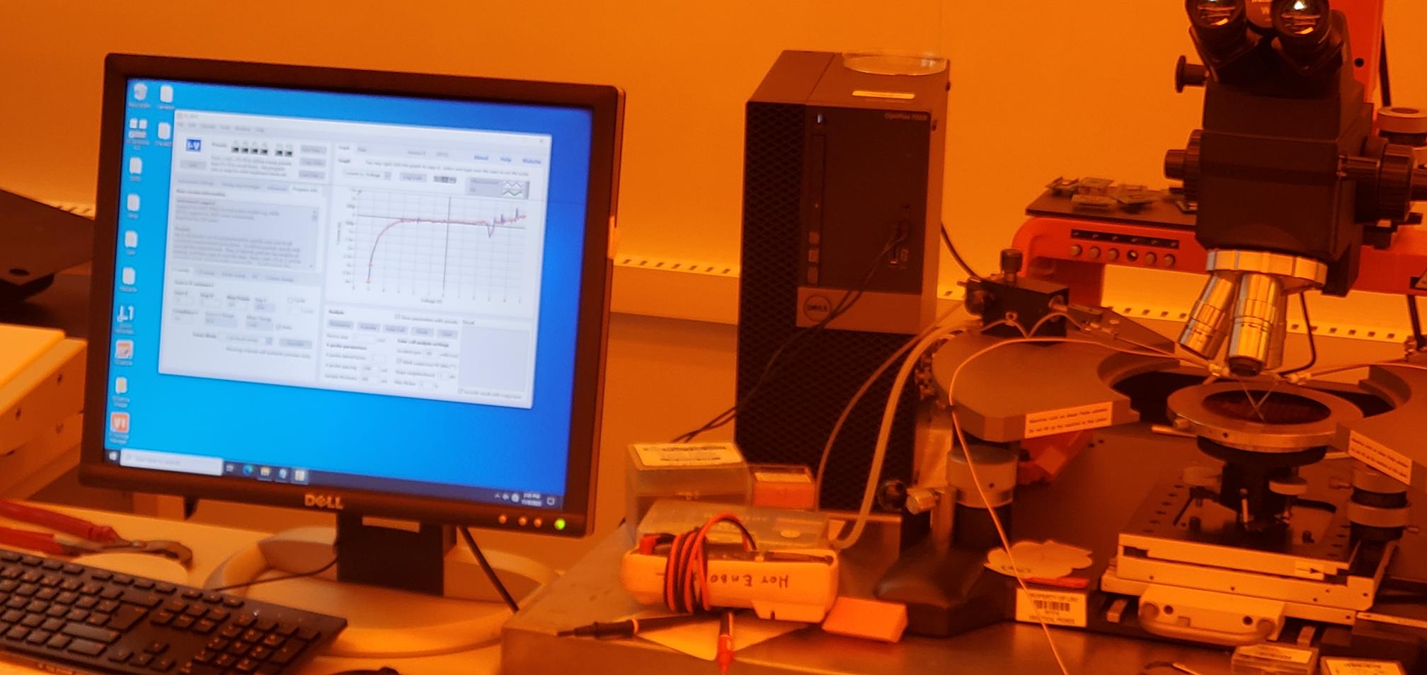 .Image 3 - Electrical Charge Data

Image 6 - AFM Scan Review
Week 10 - The final class concluded with students viewing their sample properties by SEM
.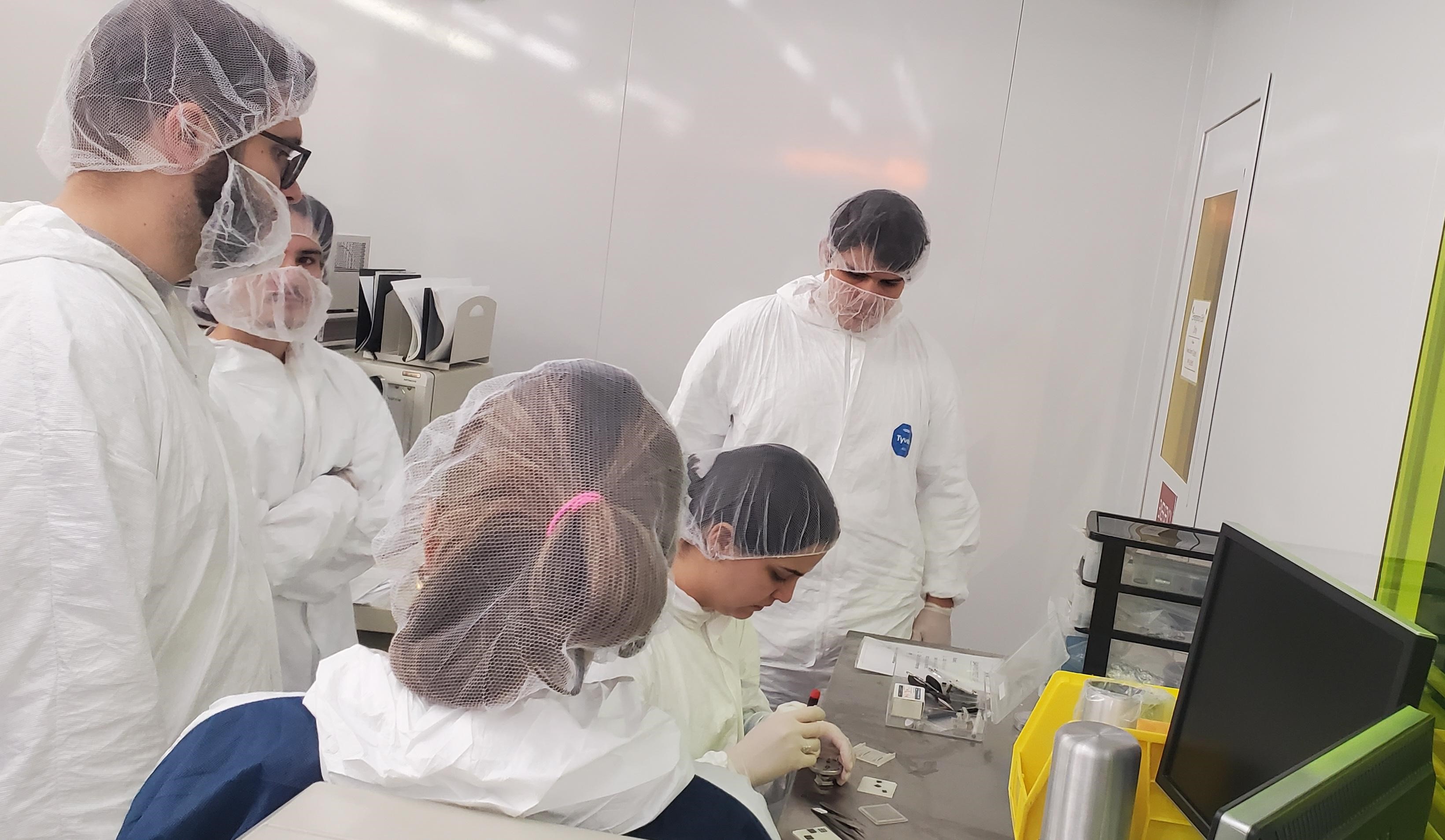
Image 1 - SEM sample prep
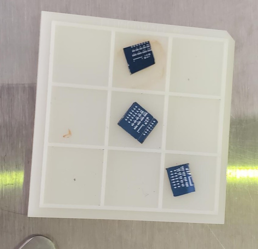
Image 2 - The Device