Spring 2024 - Chemical Engineering 4420 " Special Topics Course"
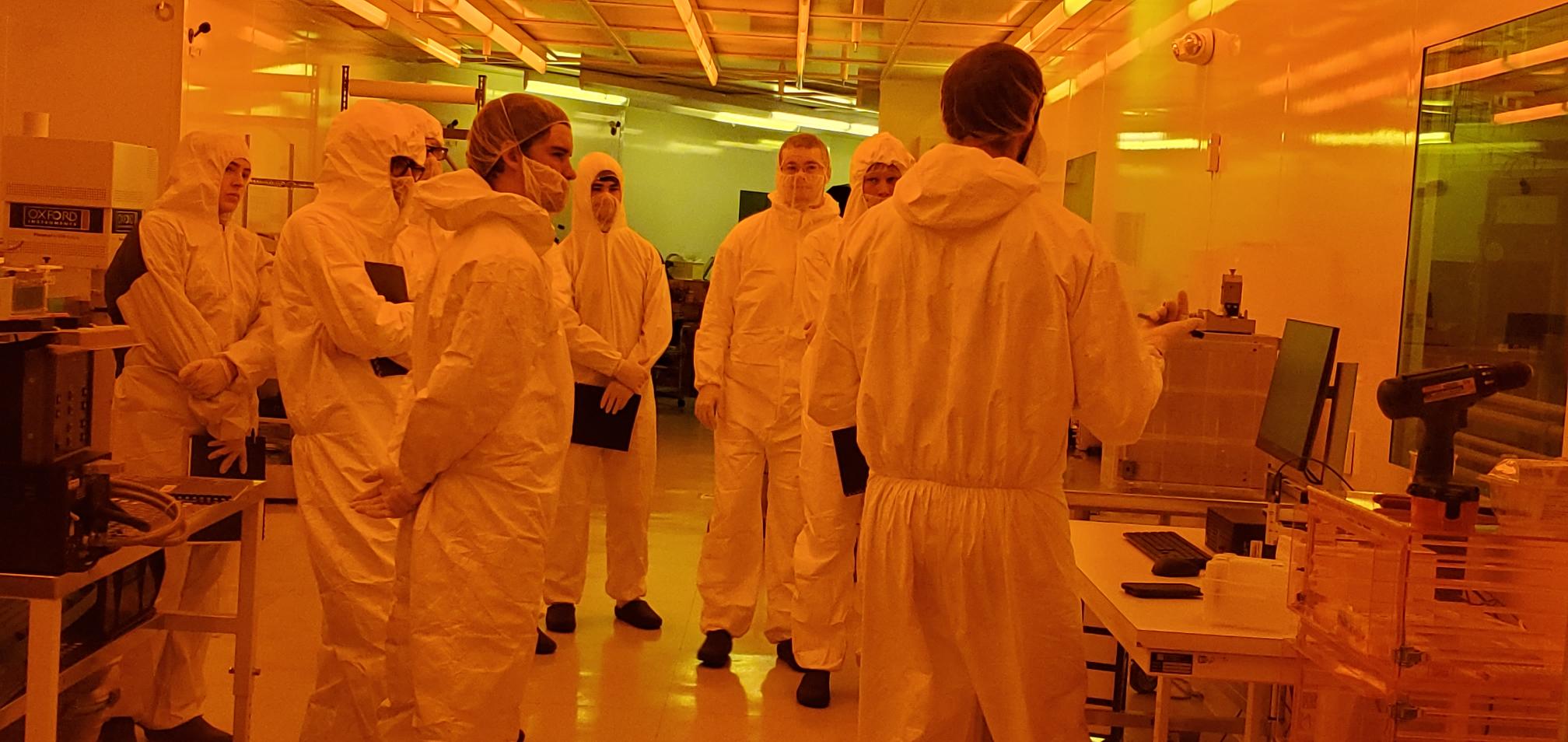
Week 1 - Students where introduced to the fundamentals of working in a cleanroom and reviewed machines that will be utilized during the course.
Week 2 - Students began with an introduction to Ellipsometry and completed test scans followed by thin film thickness measurement
.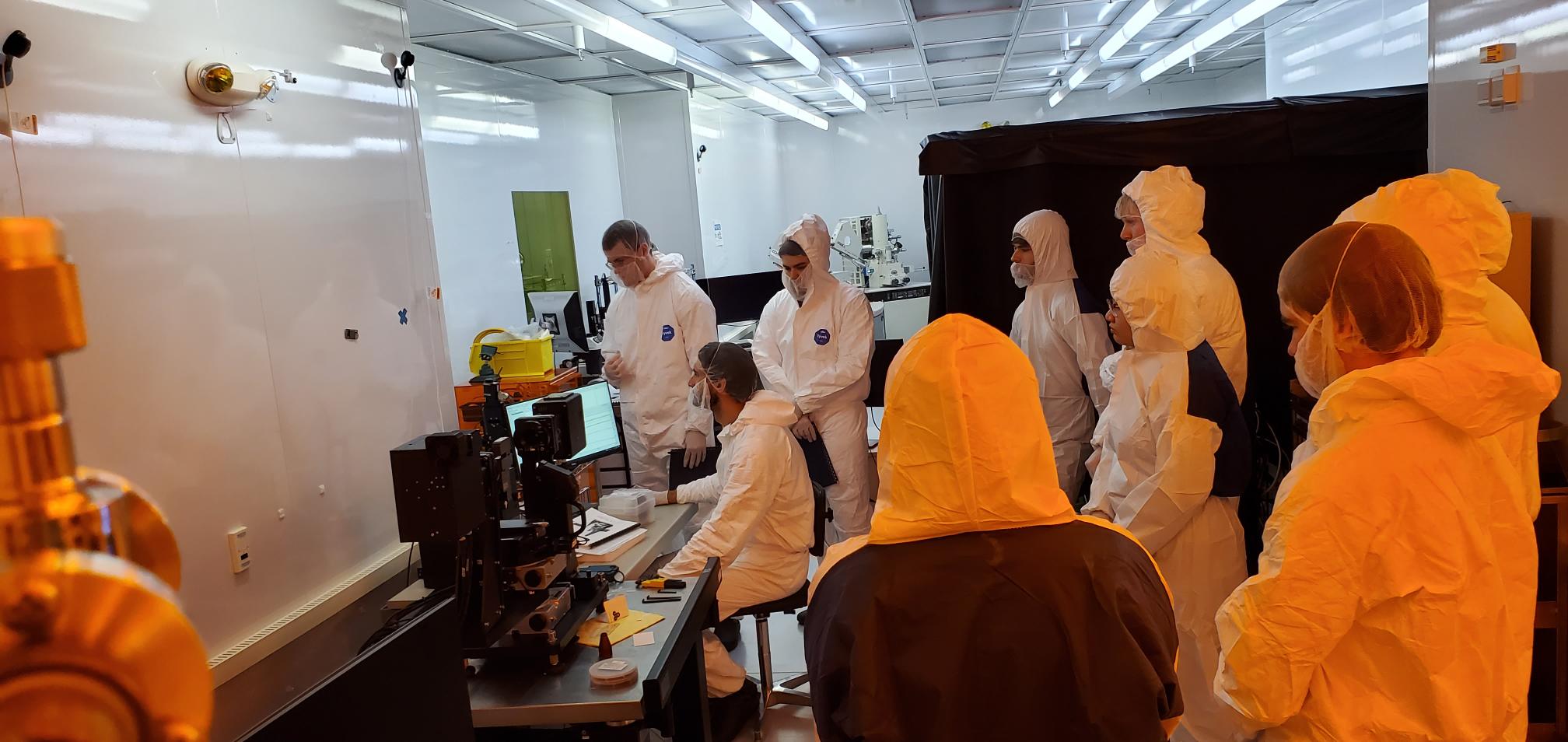
Image 1 - Intro to Ellipsometry
Image 2 - Thin Film Thickness Measurement
Week 3 - Sample preparation began with resist spincoating, first layer exposure/alignment and microscopic inspection
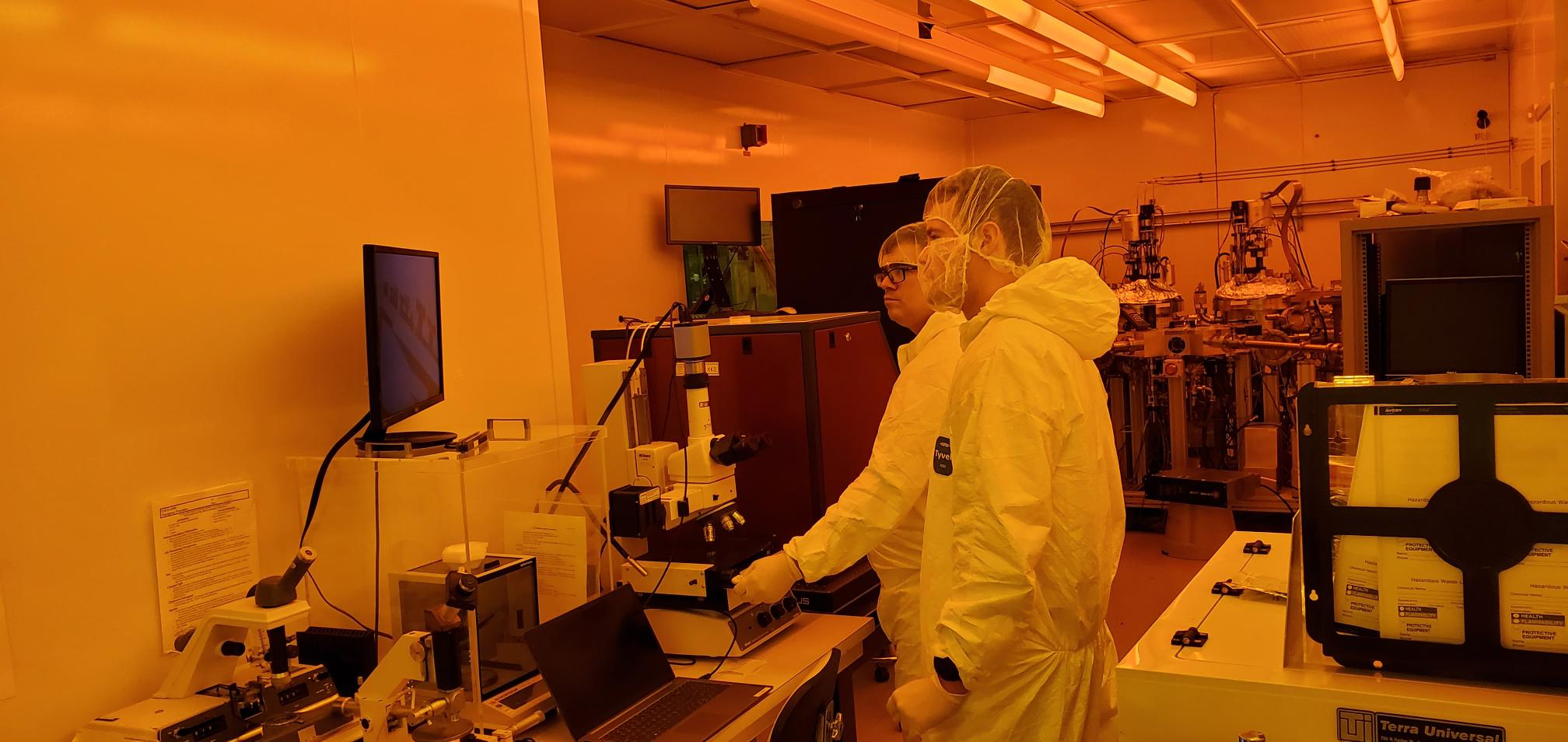
Image 1 - Microscopic Inspection
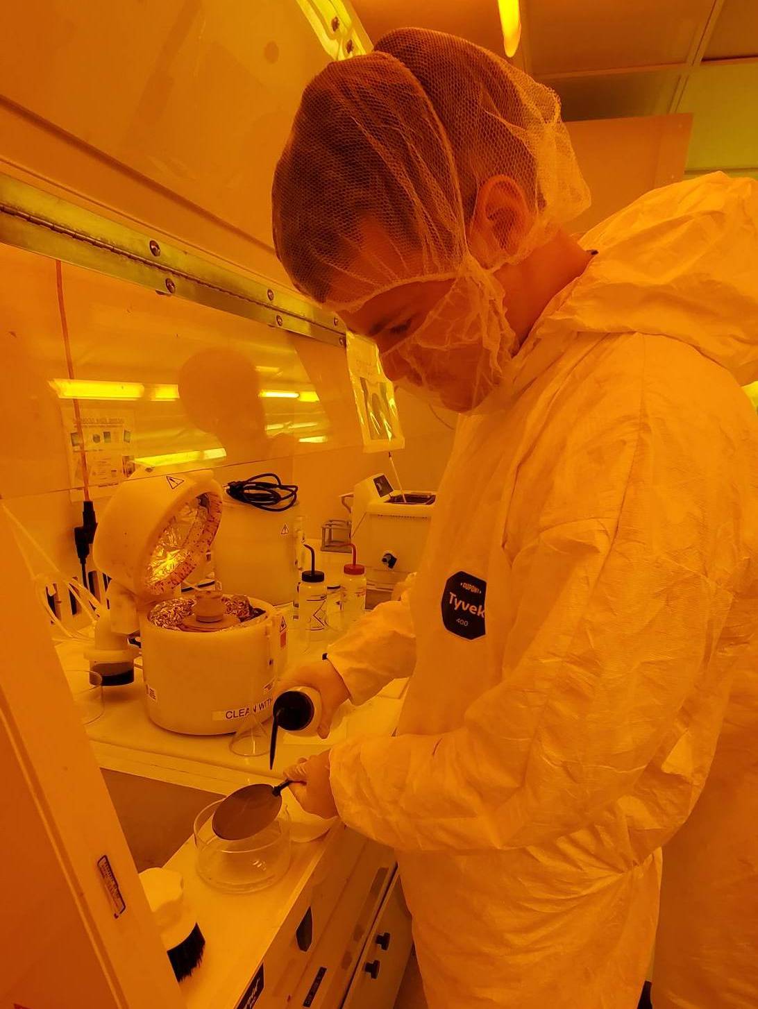
Image 2 - Sample cleaning
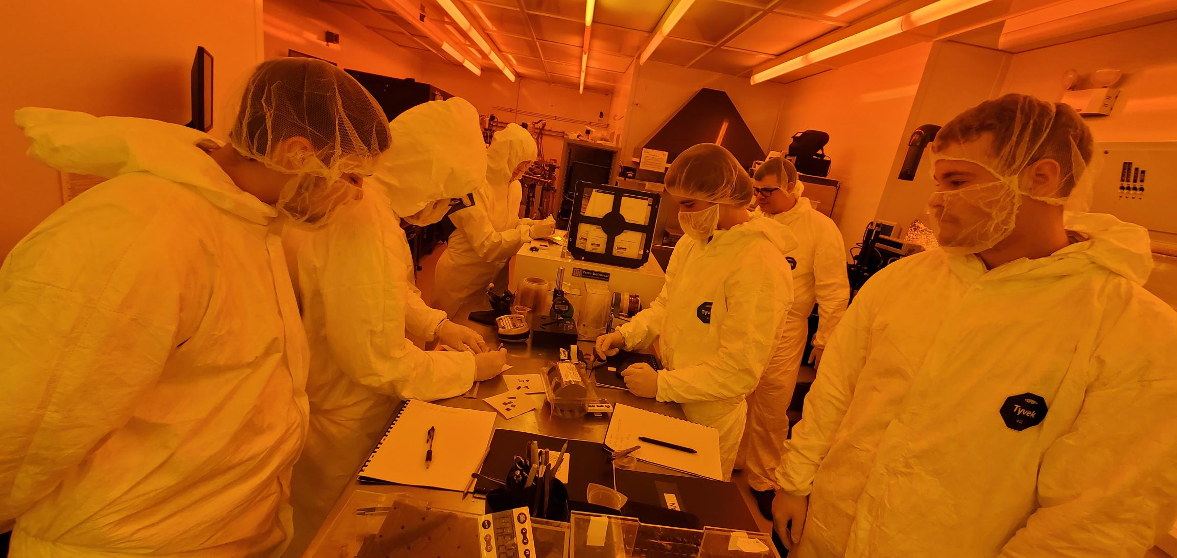
Image 3 - Sample Prep
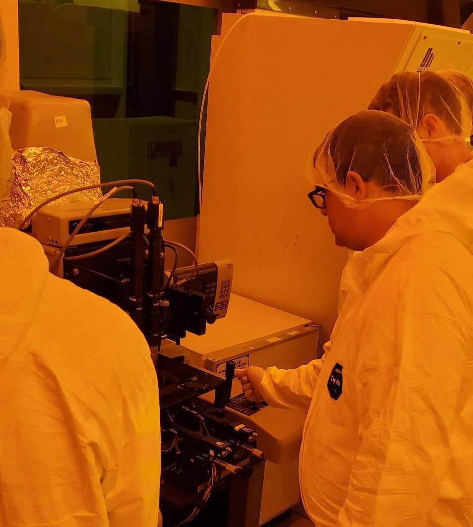
Image 4 - Exposure/Alignment
Week 4 & 5 - Students prepped samples for the dopant layer application. Next, students checked the alignment with previous markers etched in their wafers then applied the dopant layer. The organic layer of the dopant was removed by O2 Plasma then diffused into the silicon by Rapid Thermal Annealing.
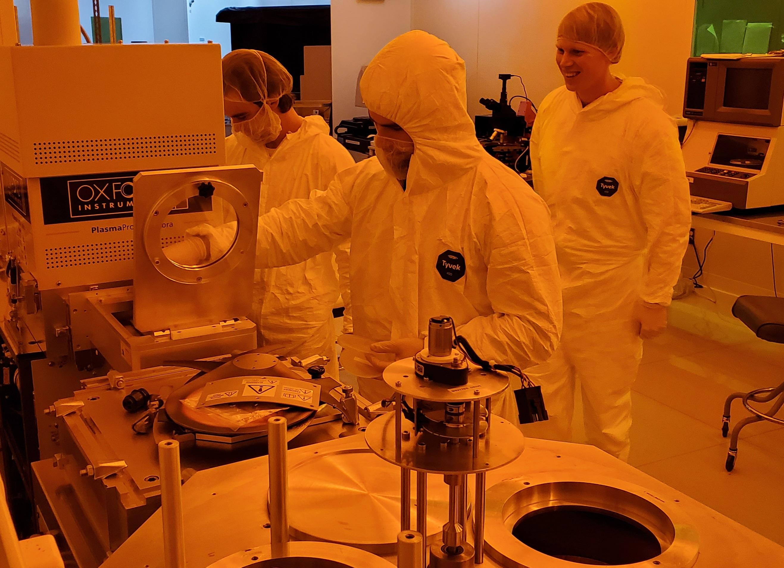
Image 1 - O2 Plasma Removal
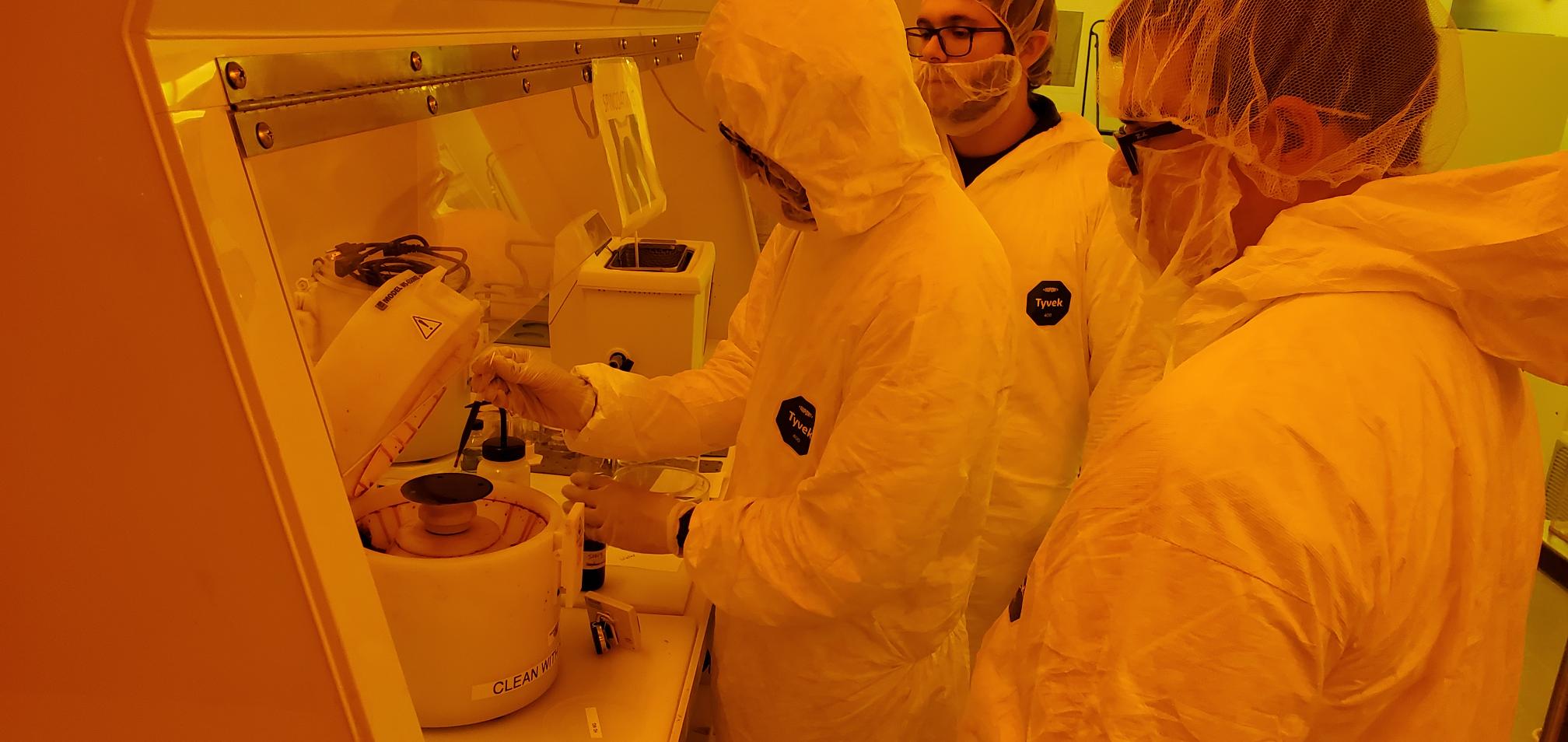
Image 2 - Dopant layer application
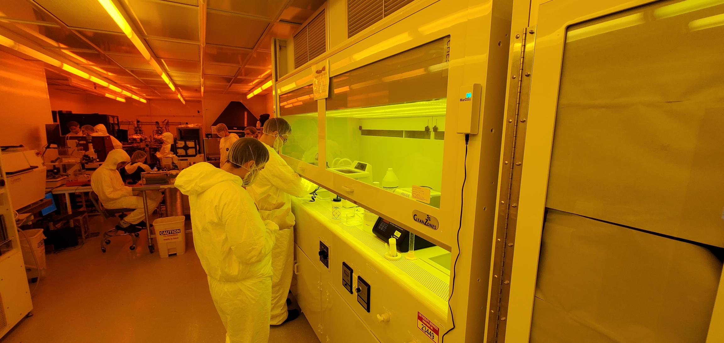
Image 3 - Development
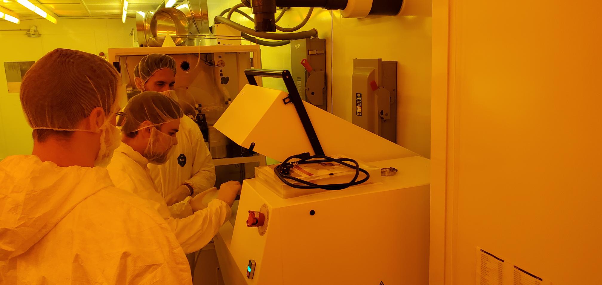
Image 4 - Rapid Thermal Annealing
Week 6 - Students etched the glass layer from their samples in preparation for application of the second layer
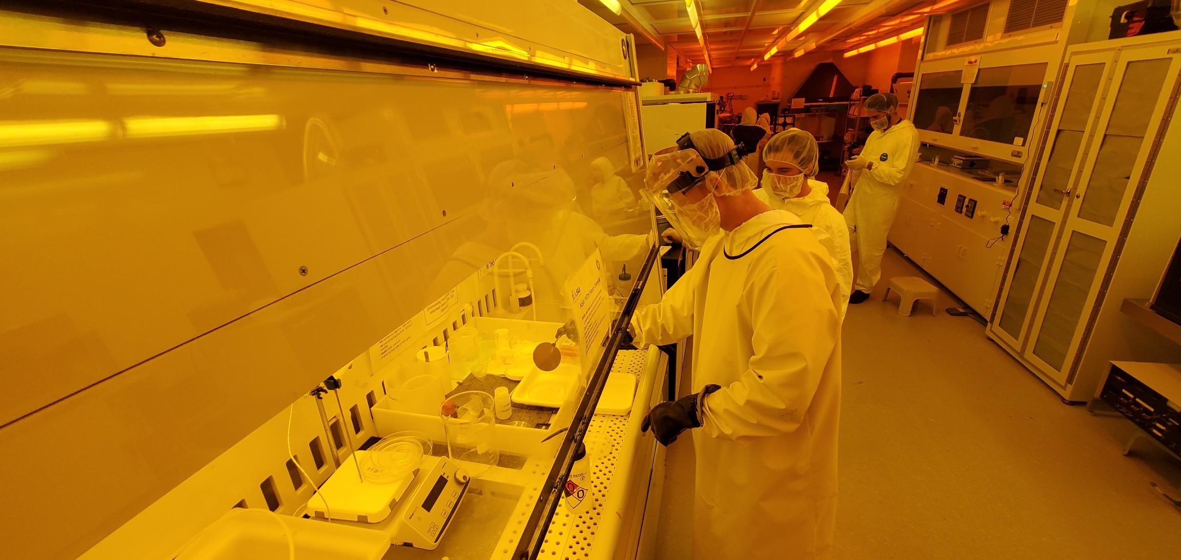
Image 1 - HF Etching
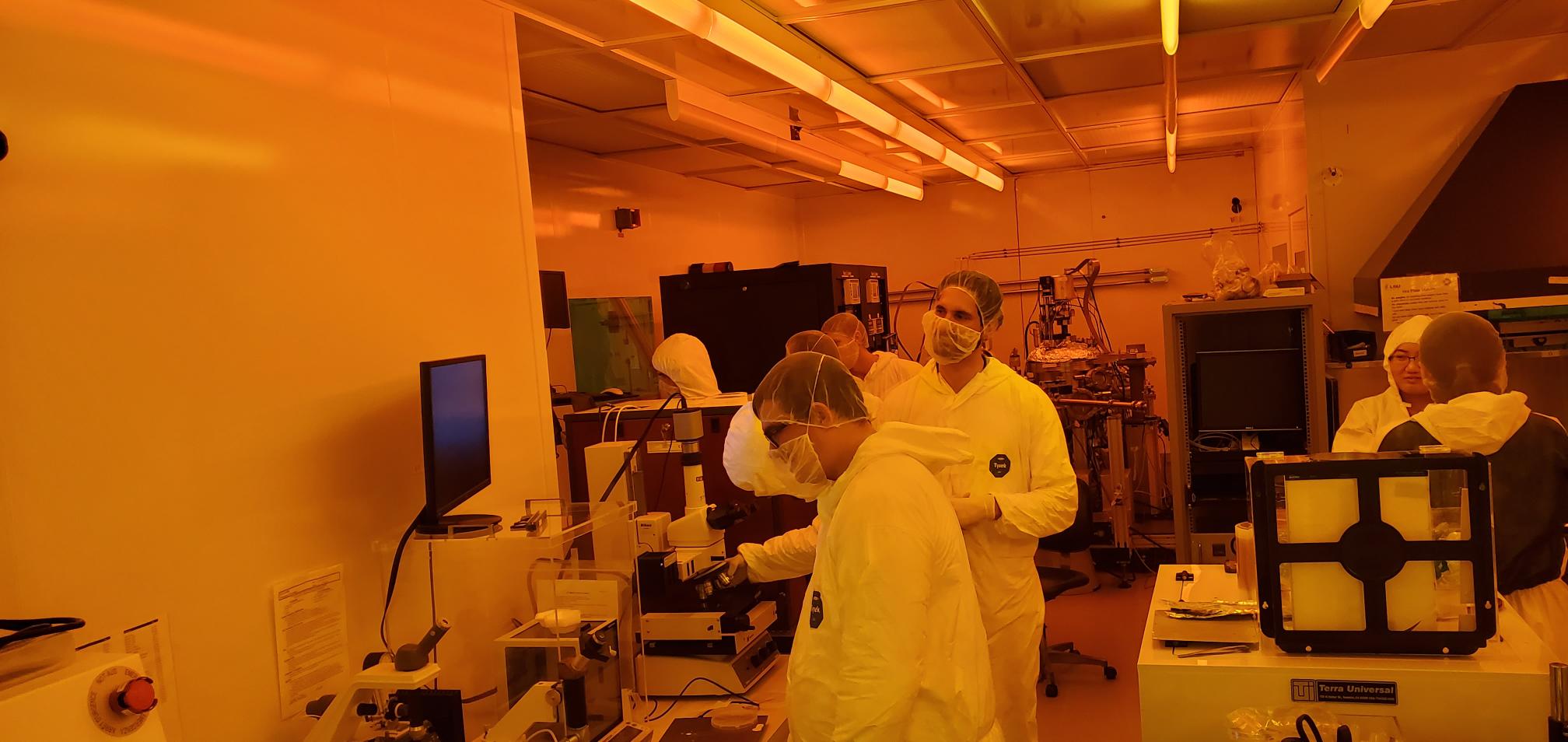
Image 2 - Microscopic Inspection
Week 7 - This week students completed the second layer application and verified both layers. The samples were prepped for the final layer
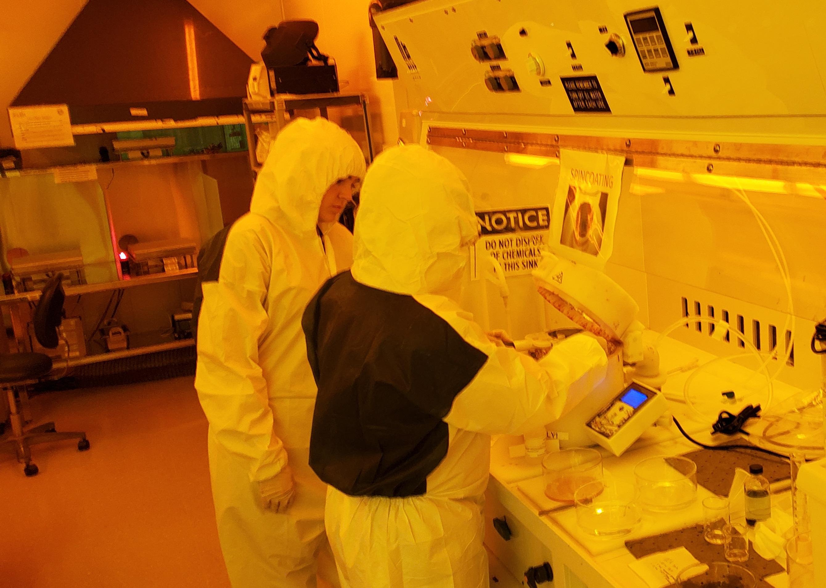
Image 1 - Resist Spincoating
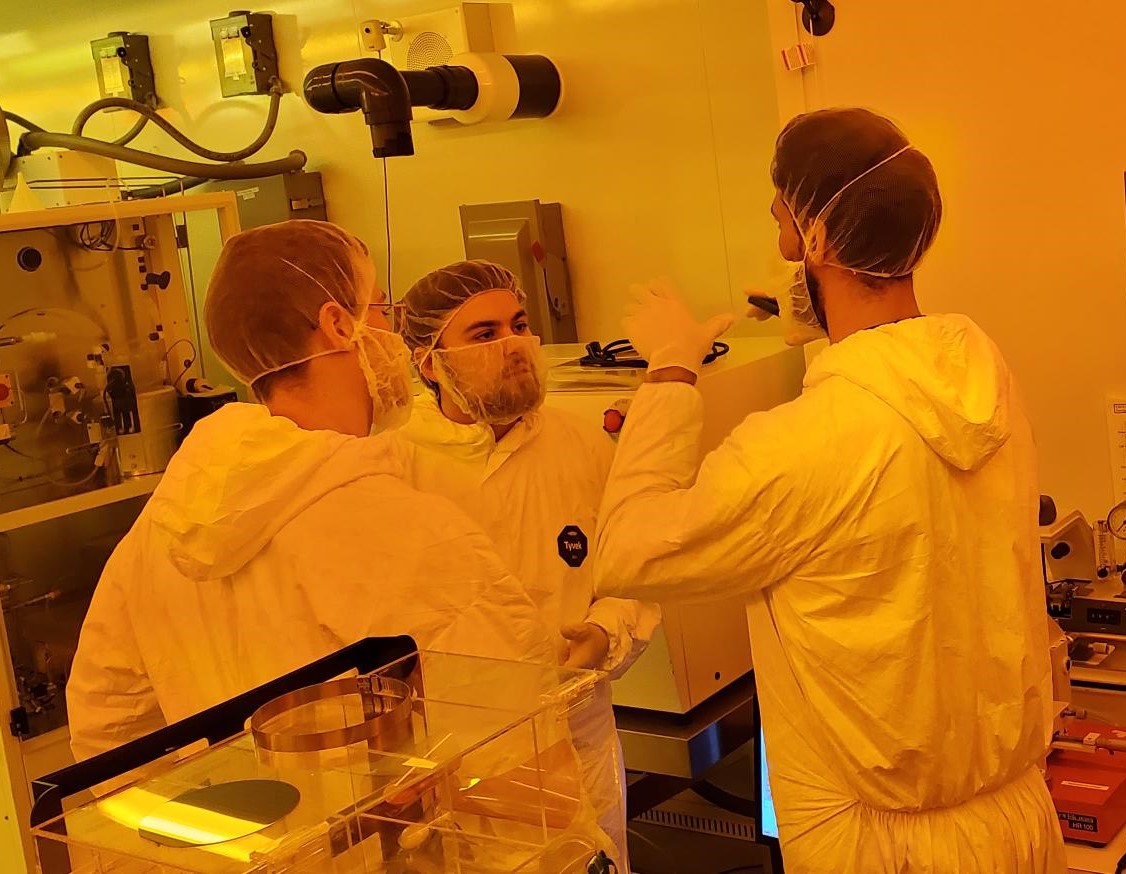
Image 2 - Class Discussion
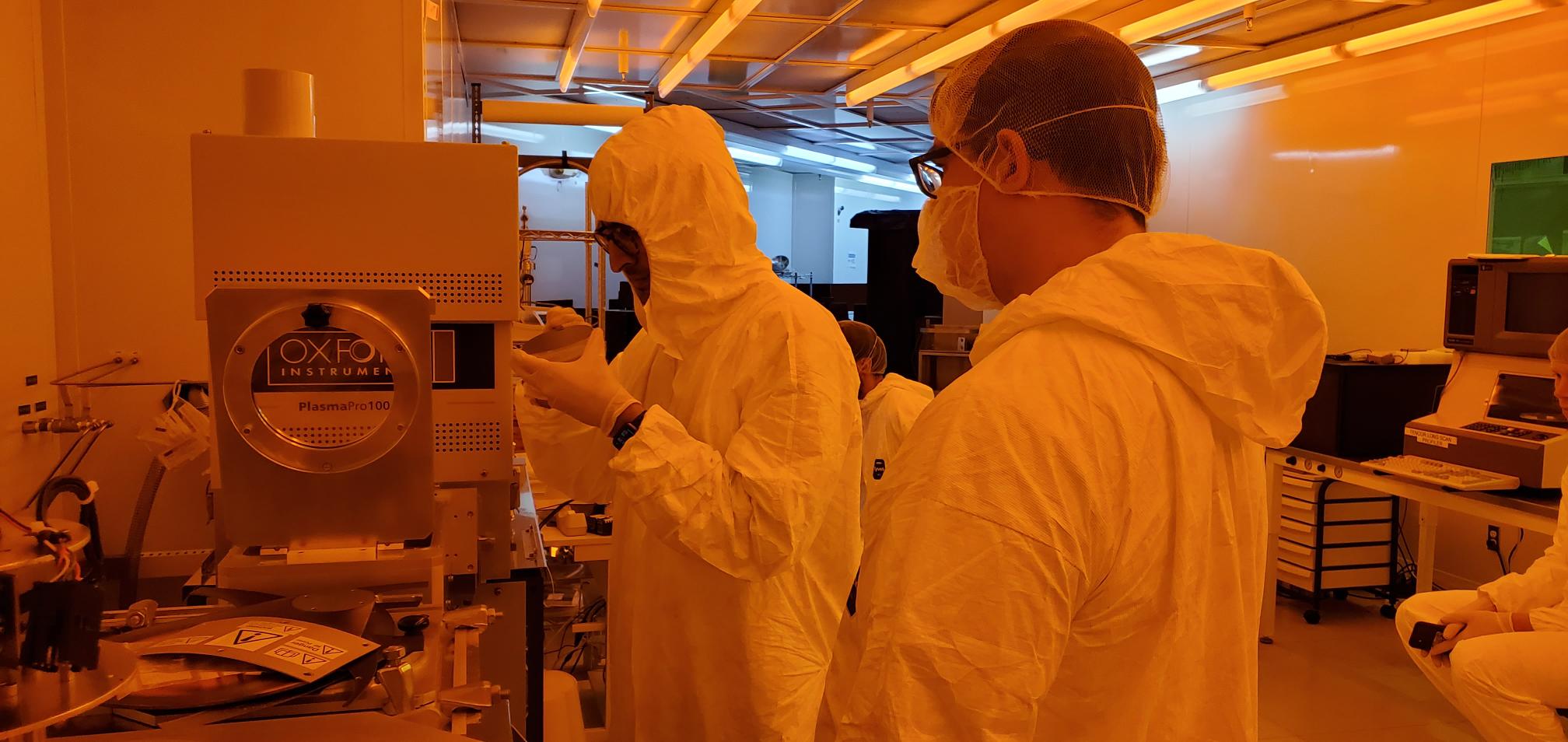
Image 3 - Second Layer Etch
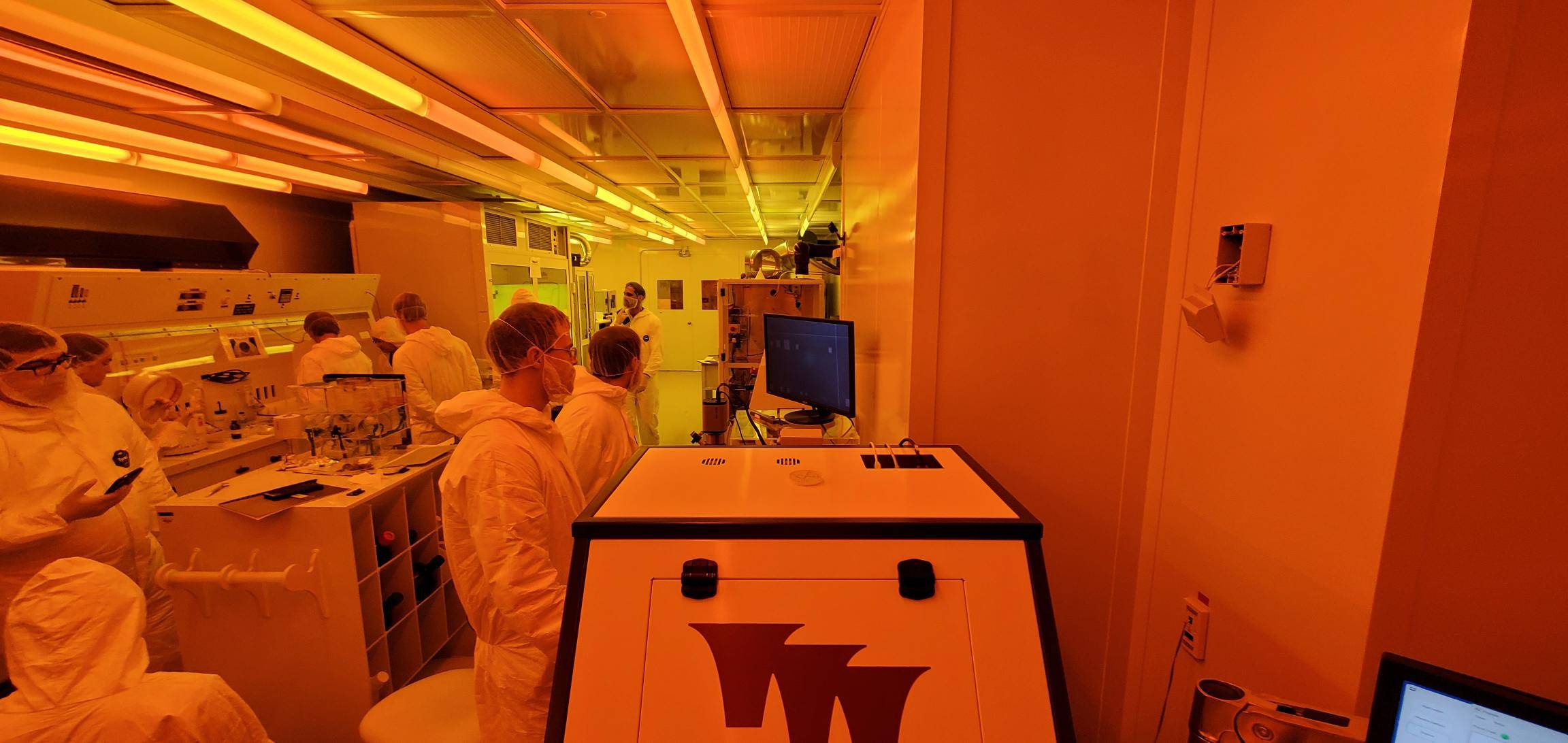
Image 4 - Microscopic Inspection
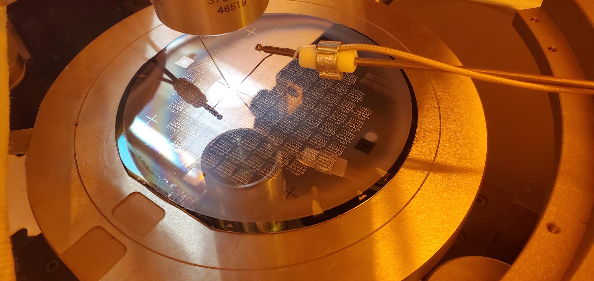
Week 8 & 9 - Students applied the final layer of their samples, deposited the final metal layer, confirmed an electrical current then measured the electrical properties by AFM
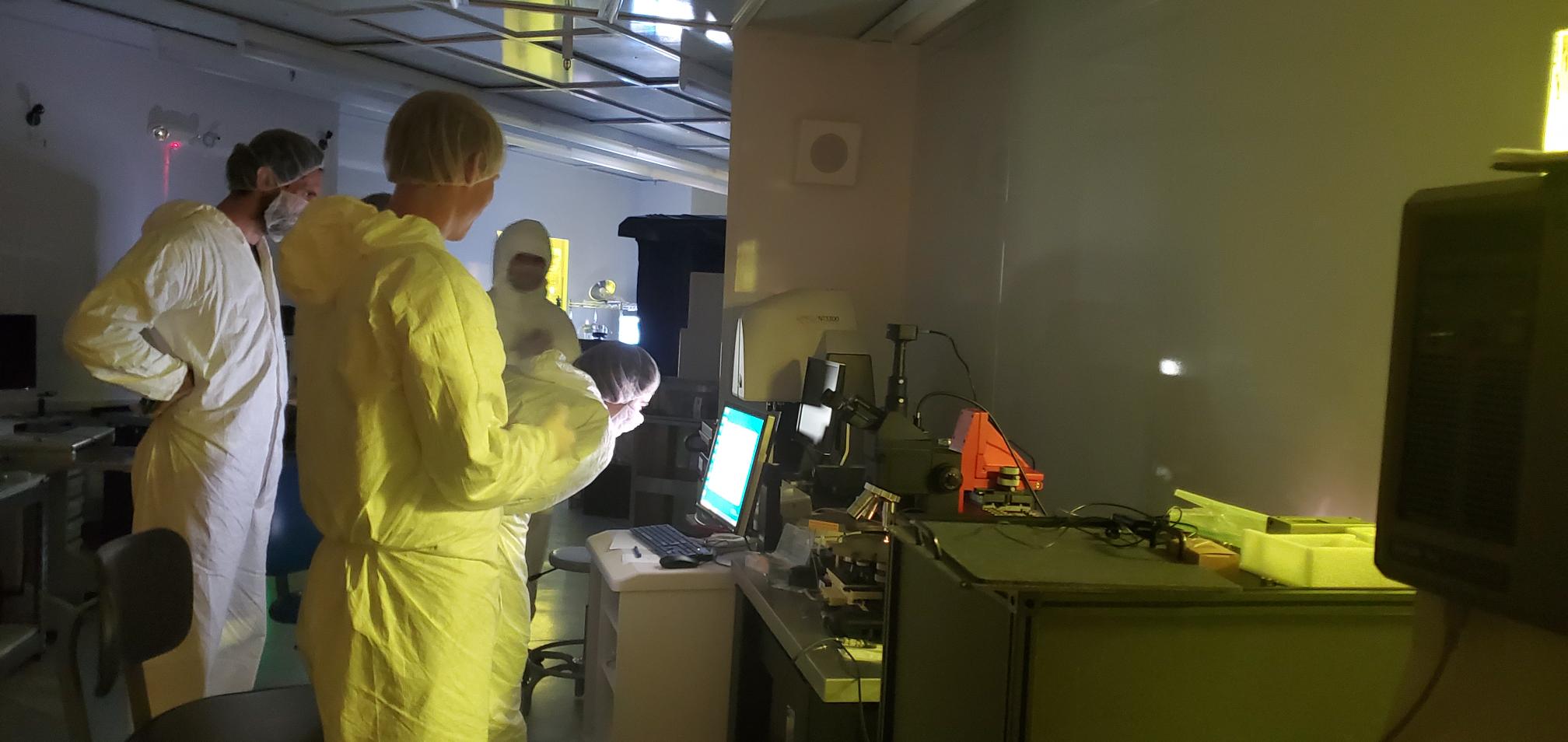 Image 1 - Probe Station
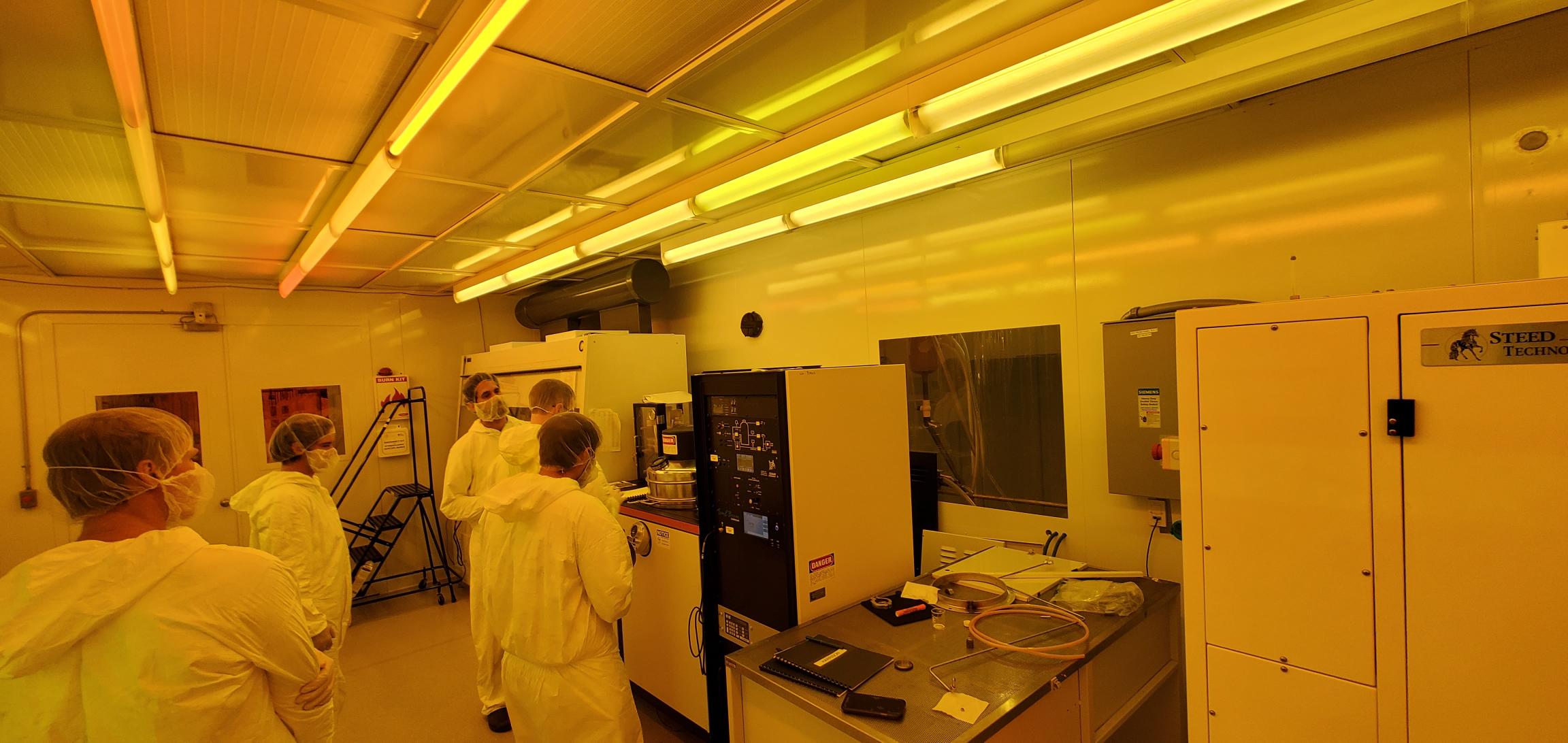 Image 2 - Ebeam Metal Layer Deposition
.
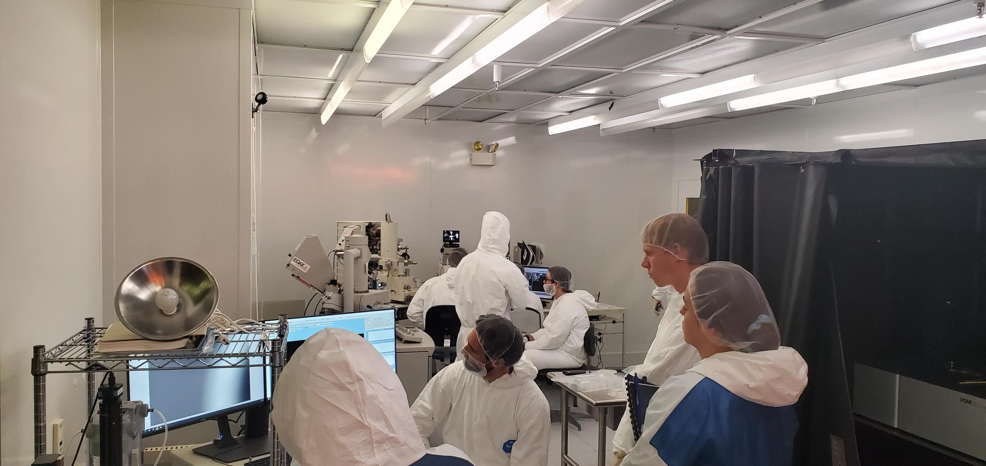
Image 3 - AFM
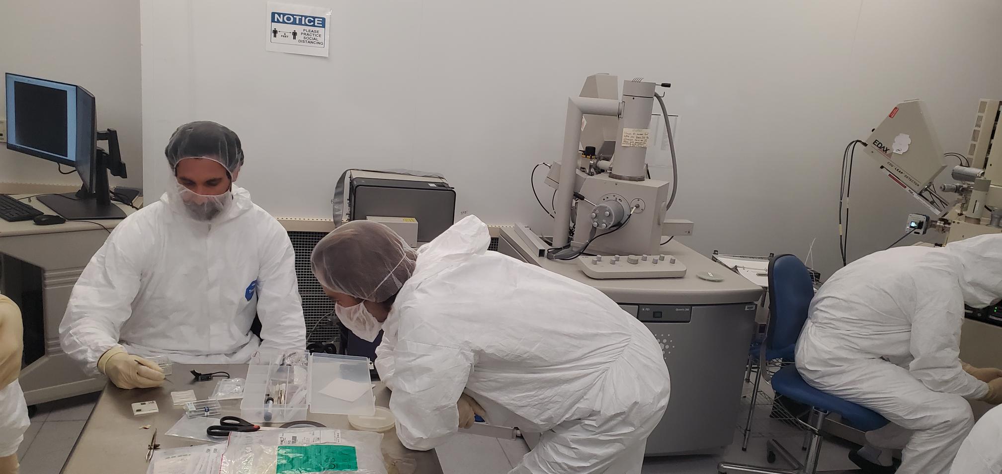
Image 4 - AFM Sample Prep
Week 10 - Students completed the last step to device fabrication by collecting charge data from their newly fabricated devices.