Spring 2023 - Chemical Engineering 4420 "The Steps to Device Fabrication"
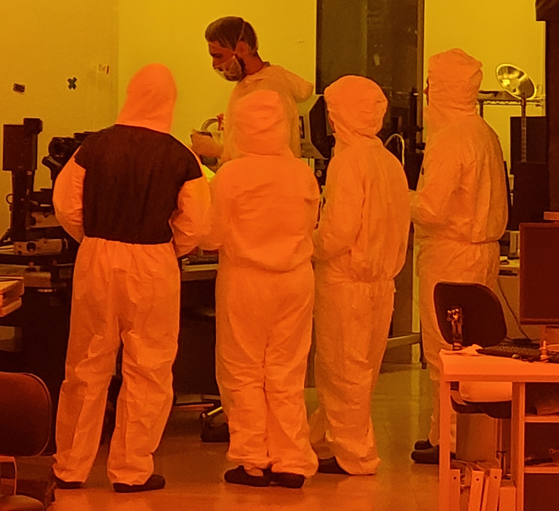
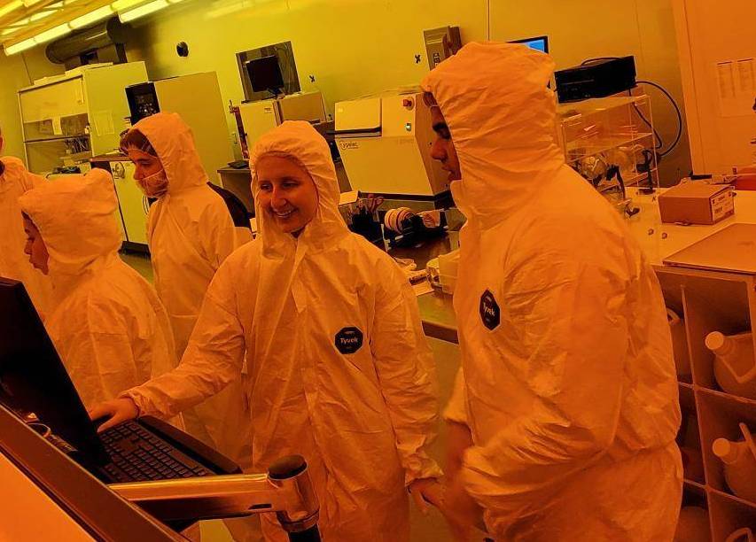
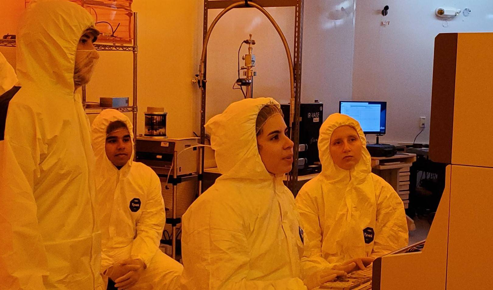
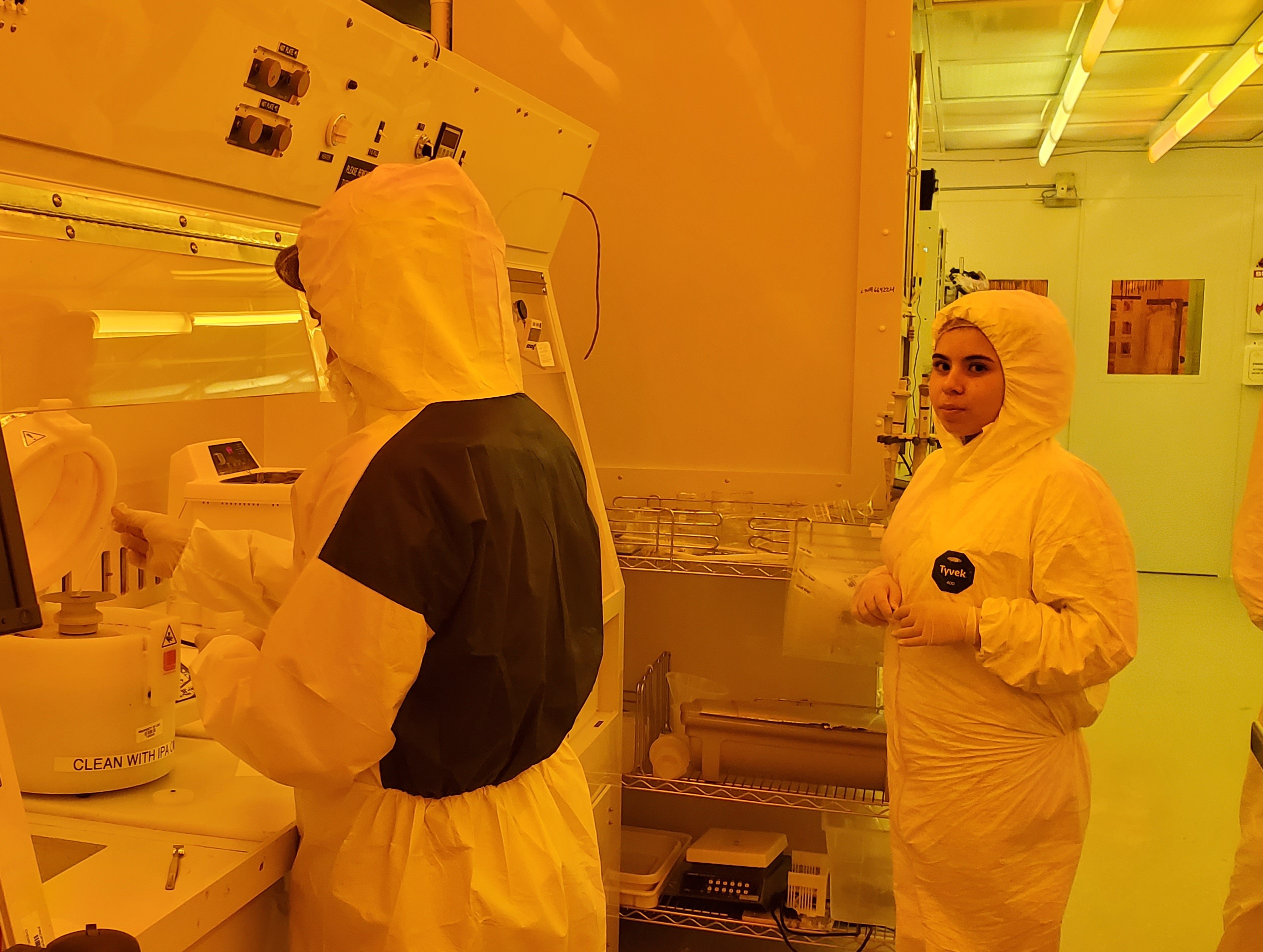
Week 1 - "Introduction to the Nanofabrication Facility"
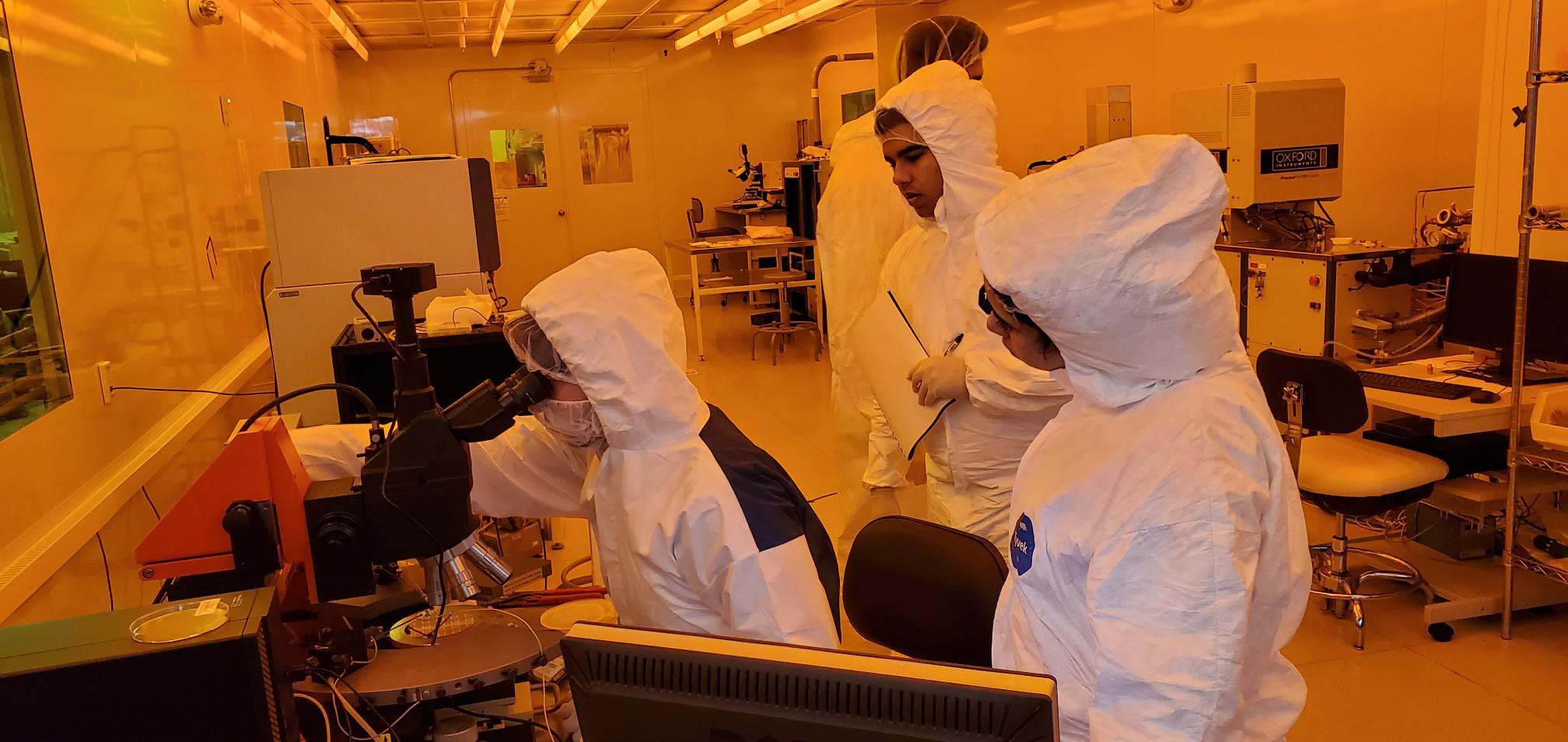
Dr. Lendinez discusses the basics of cleanrooms and reviews the fleet of tools at the NFF.
 .
.
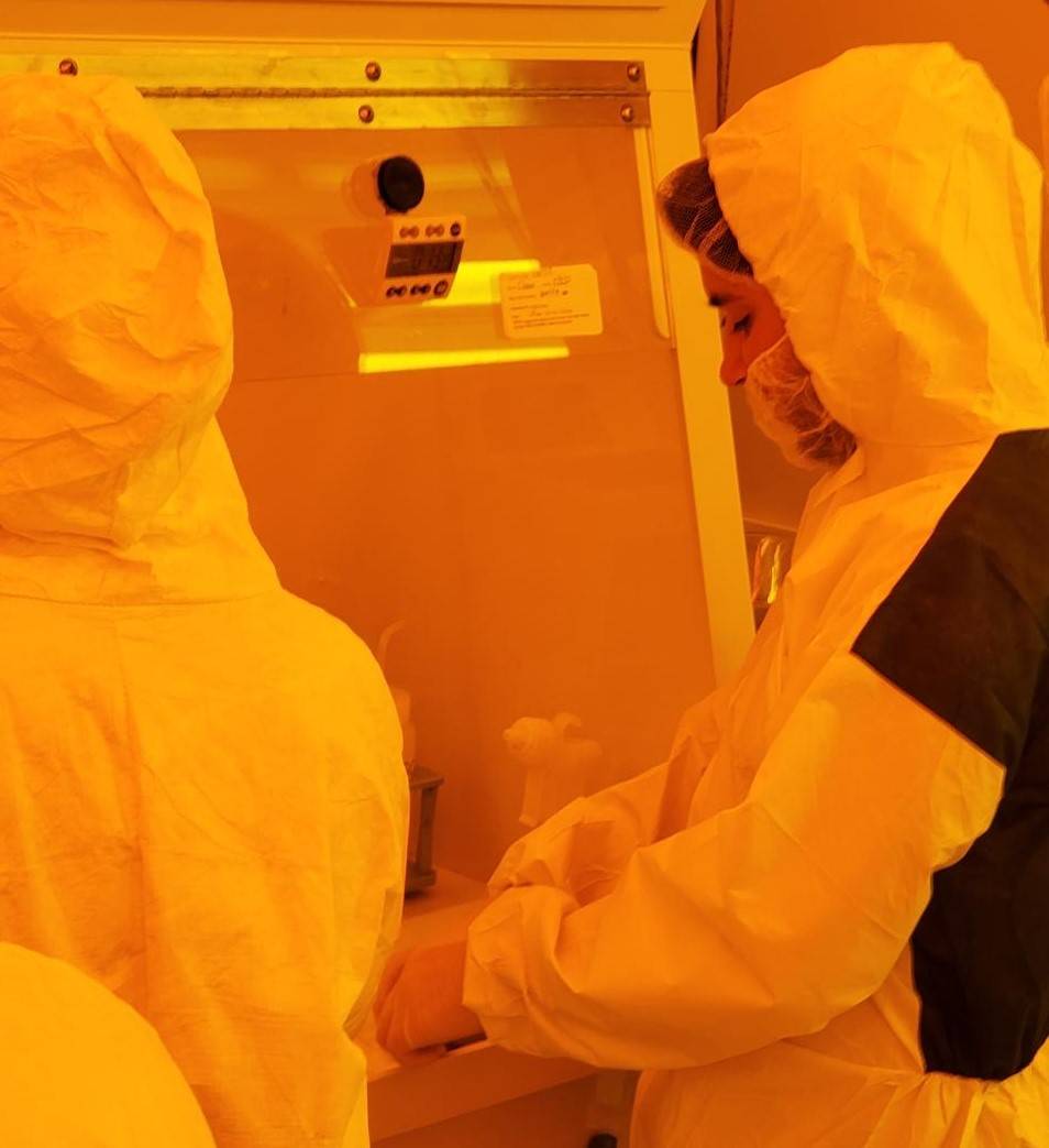
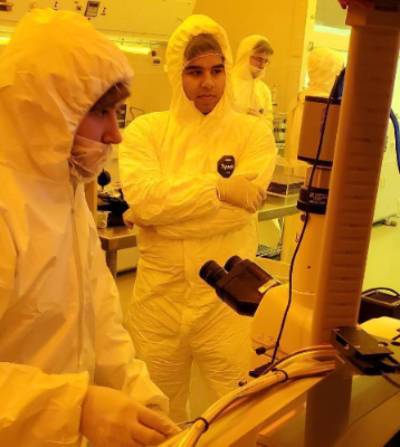
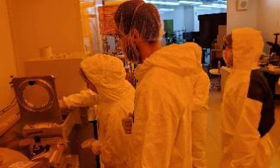
Week 2 - "Ellipsometry"
Students collected Ellipsometry data using the Woollam RC2 from silicon substrates coated with SiO2 followed by resistivity measurements
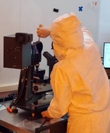
image 1- Sample Placement
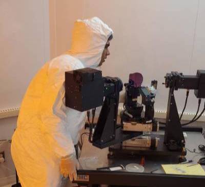
image 2- Alignment
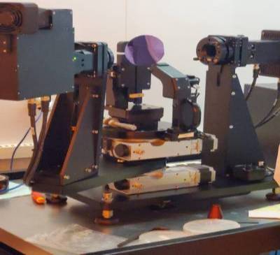
image 3- Scanning
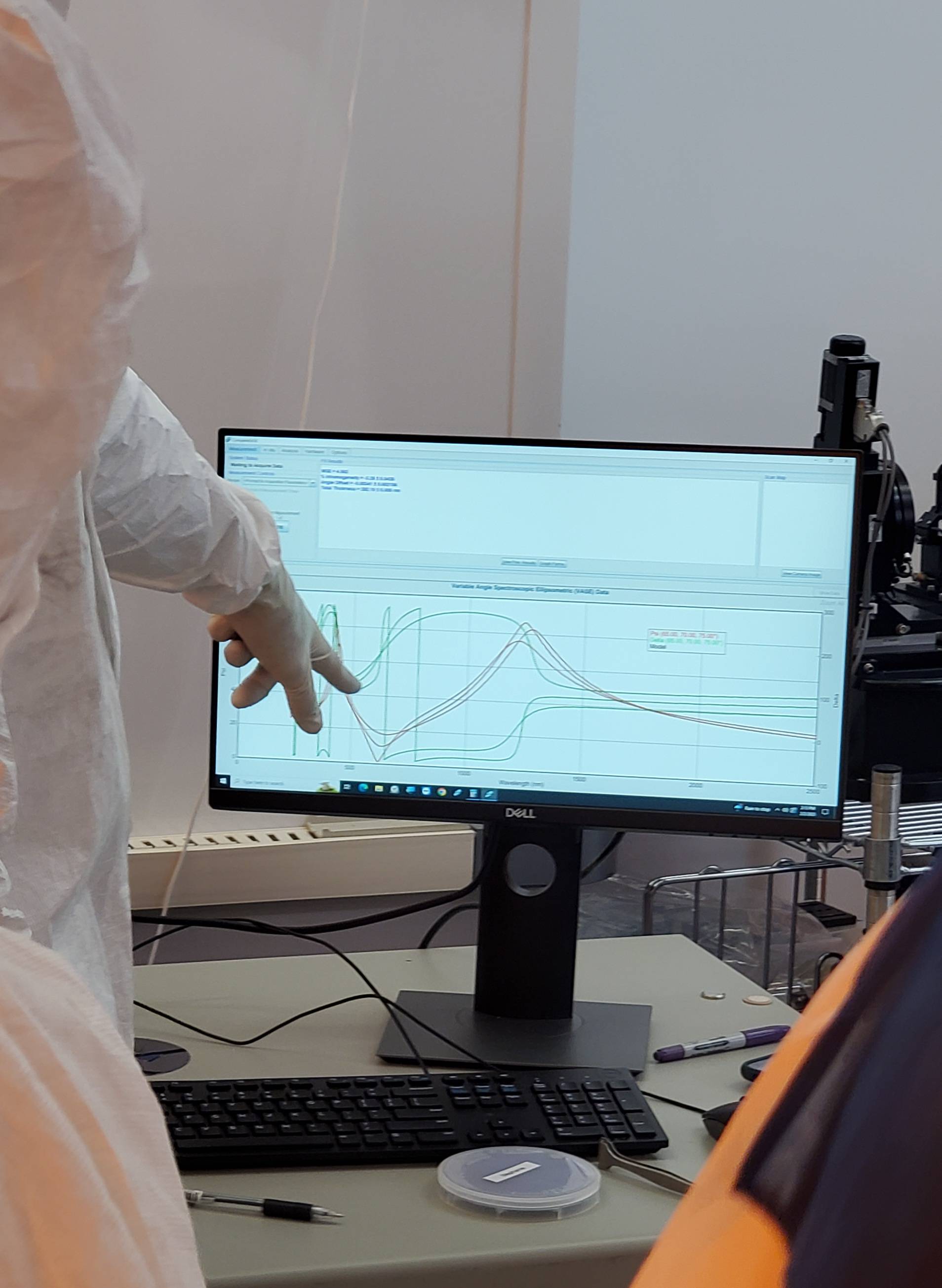
image 4 - Data Collection
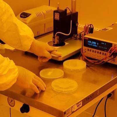 . image 5 - Resistivity Measurements
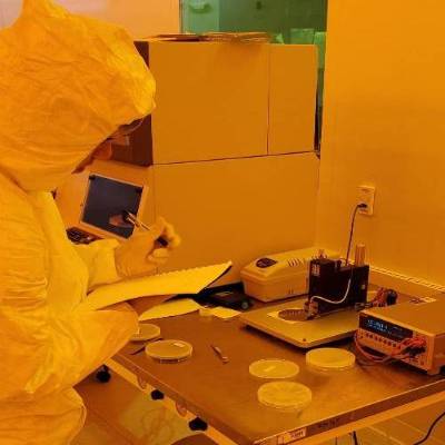 .image 6 - Recording Resistivity Data
Week 3 - "First Layer Preparation"
Students began the first steps to device fabrication. Markers were etched on to silicon wafers to ensure samples are properly aligned throughout the entire process. This hands on practical provided students the opportunity to actively apply the steps discussed from the third week's lecture while gaining knowledge of machinery aiding in the fabrication process.
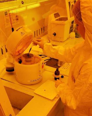
Step 1- RCA + Ultrasonic Cleaning
Step 2 - Mask Patterning Alignment Marks
Step 3 - Spincoating Photoresist
Step 4 - Soft Bake
Step 5 - Resist Development
Step 6 - Microscopic Inspection
Step 7 - DRIE (Thermal Oxide Etch)
Step 8 - Etch Depth Profiler Scan
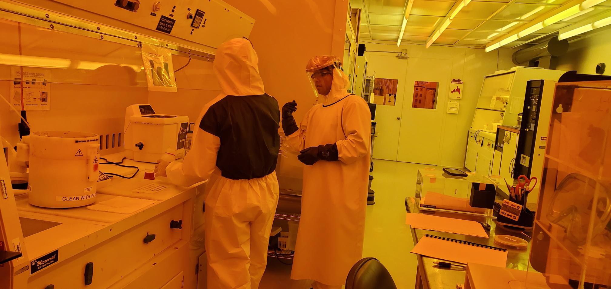
Week 4 - " Dopant Layer Preparation"
This week students patterned openings through the SiO2 in order to apply the dopant layer for next weeks' session. An oxygen plasma source was used to remove excess organic residue from substrates followed by S1813 resist coating. Next, students checked the alignment with previous markers etched in their wafers and exposed using the Quantum ML3Pro then development. Lastly microscopic inspection verified patterns were properly exposed and fully developed resulting in sharp edges and the presence of resistor meanders.
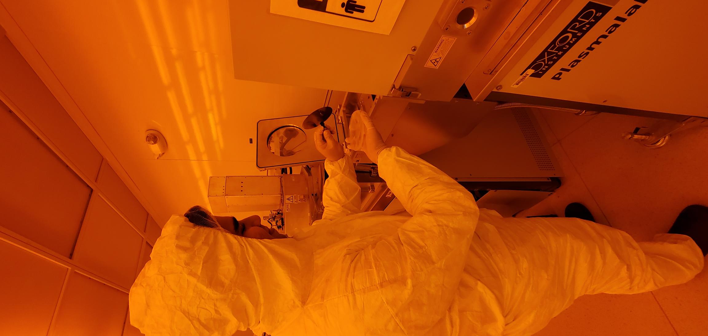
image 1 - Oxygen Plasma
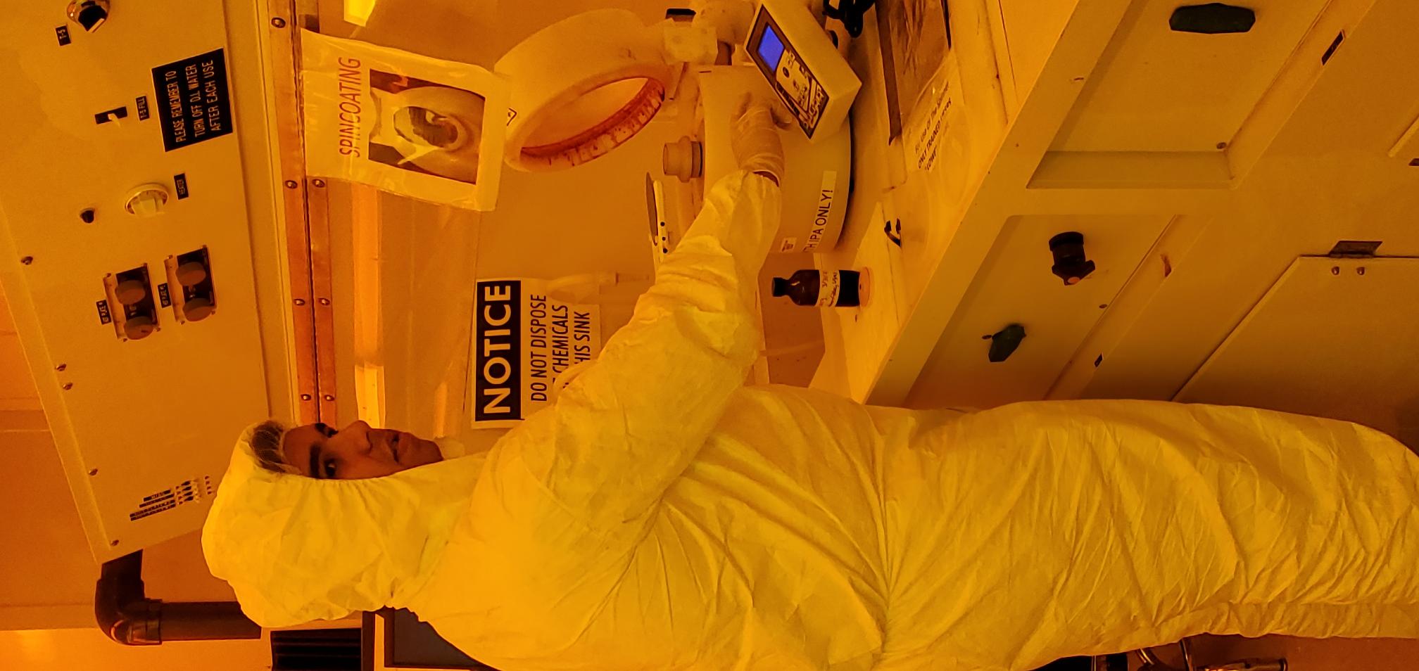
image 2 - Resist Coating
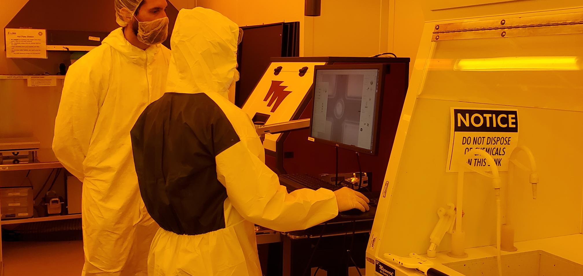
image 3 - Alignment & UV Exposure
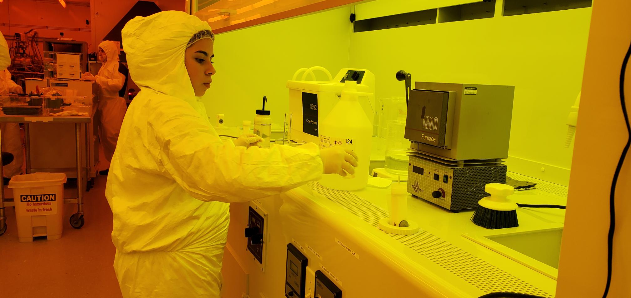
image 4 - Development
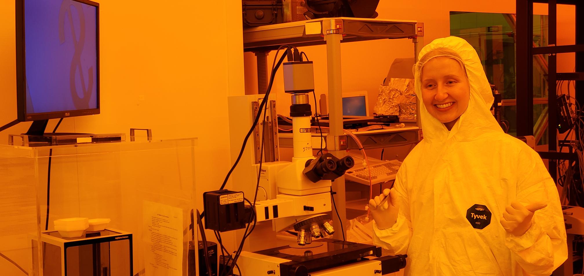
image 5 - Microscopic Inspection
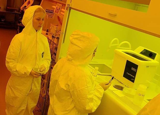
Week 5 - "Spin on Dopant"
Students etched through the holes patterned during last week's session then doped the silicon wafers in the opened areas. Silicon Oxide was etched using RIE, resist removal with acetone, followed by RCA cleaning then a soft bake to dehydrate the sample. Wafers were then spin coated with a Spin-On-Dopant (SOD) and cured. The organic layer of the dopant was removed by O2 Plasma then lastly diffused into the silicon by Rapid Thermal Annealing.
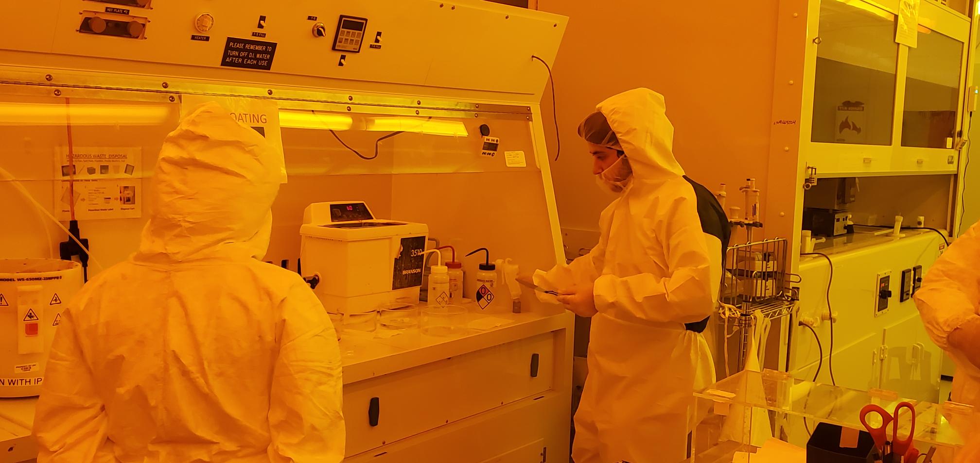
image 1 - Dopant Layer Prep
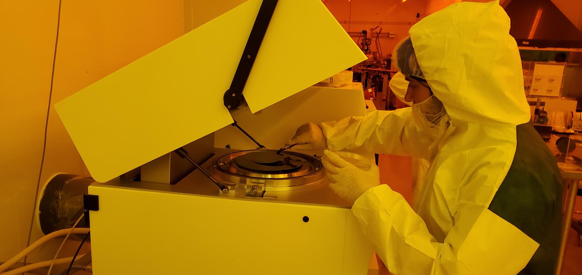
image 2 - Rapid Thermal Annealing
.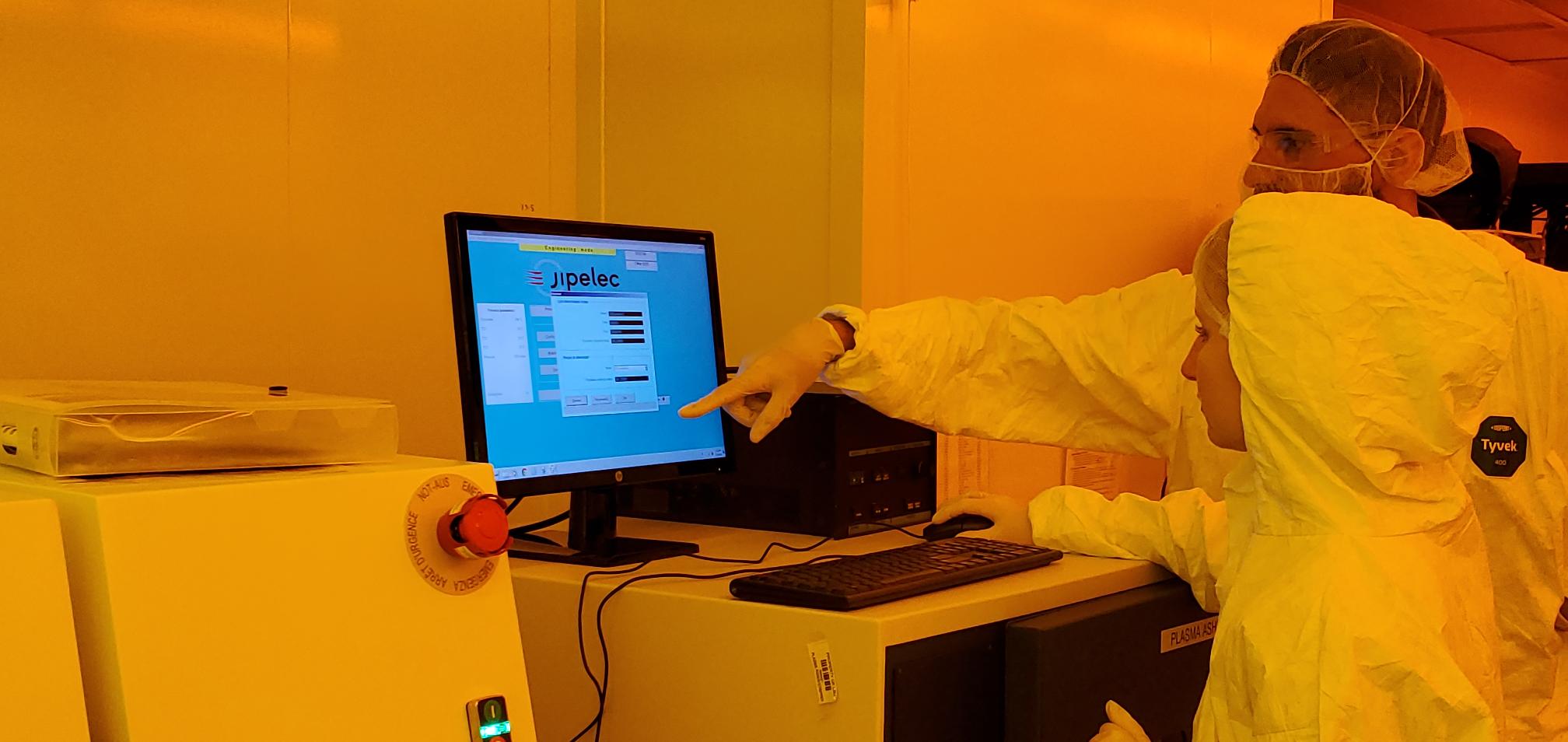
image 3 - Annealing Data
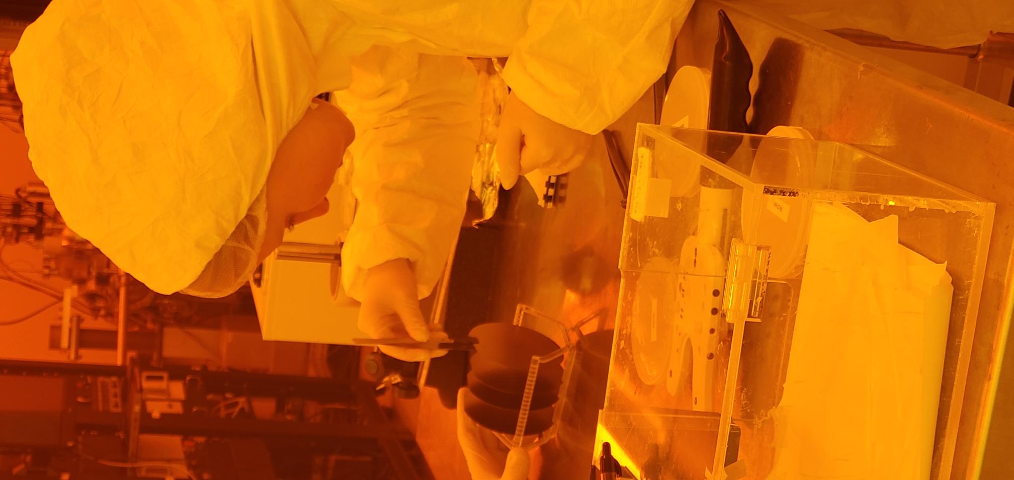
image 4 - SOD Removal
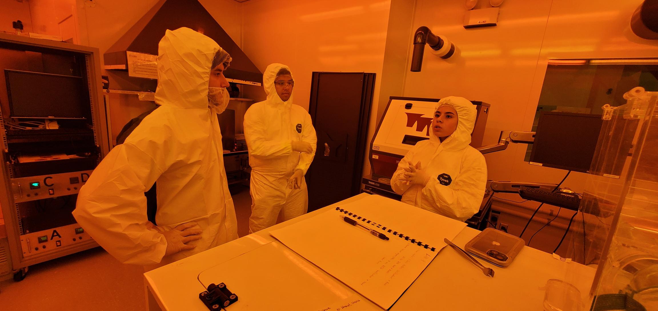
image 5 - Class Discussions
Week 6 - "Glass Layer Etching"
Students began the etch process to remove the glass layer from their samples with Hydrofluoric Acid followed by microscopic inspection. After multiple etch cycles, the glass layer was completely removed in preparation for application of the second layer in next week's class.
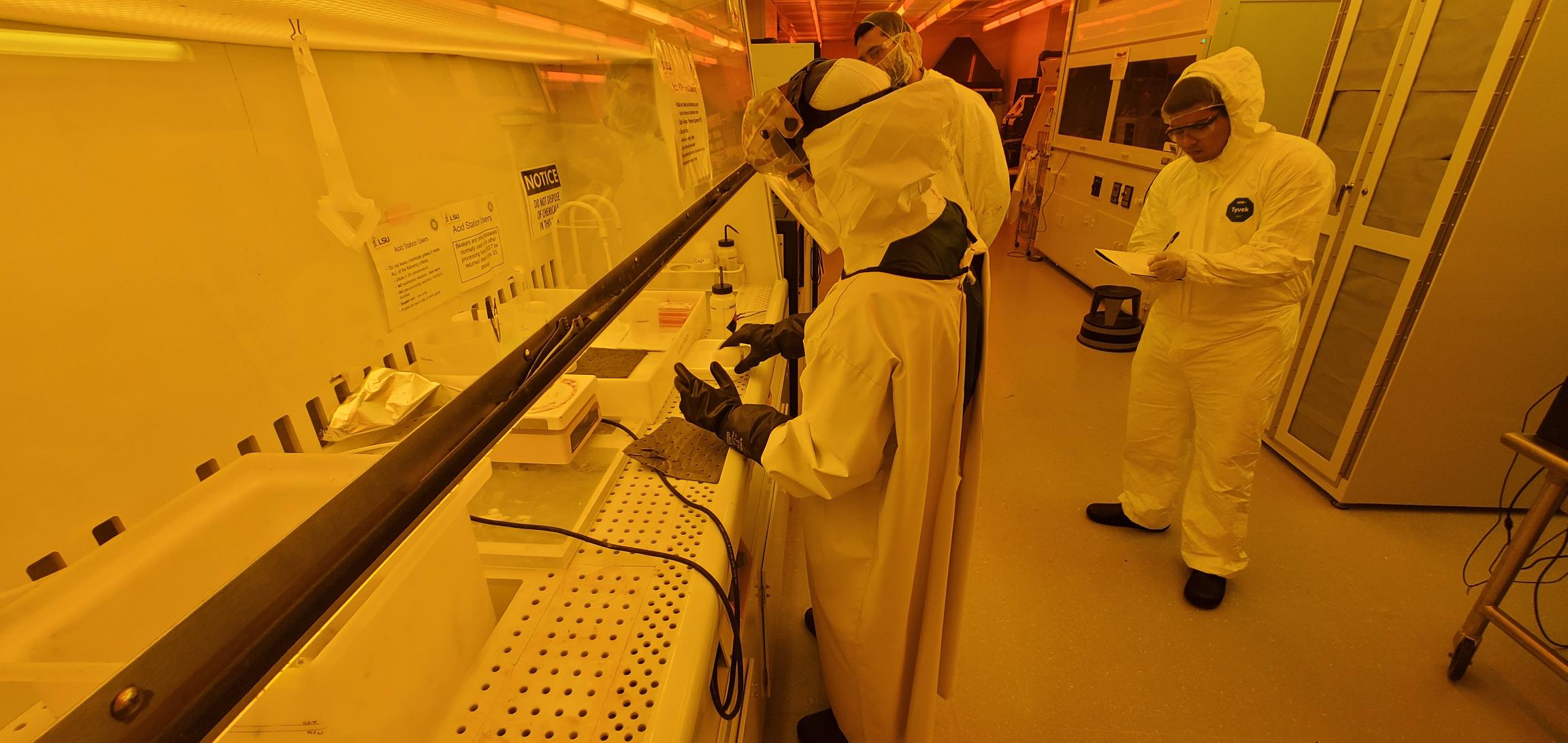
image 1 - HF Etching
.image 2 - Post HF Cleaning
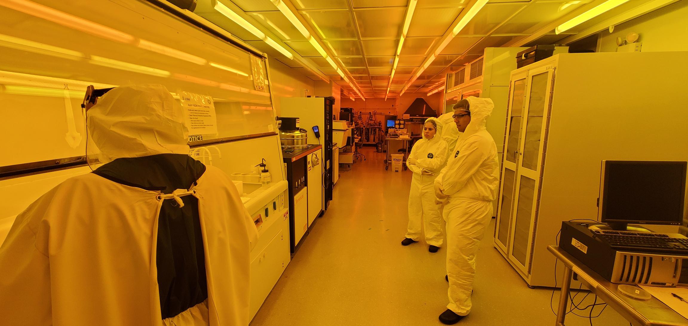
image 3 - Class Observation
.
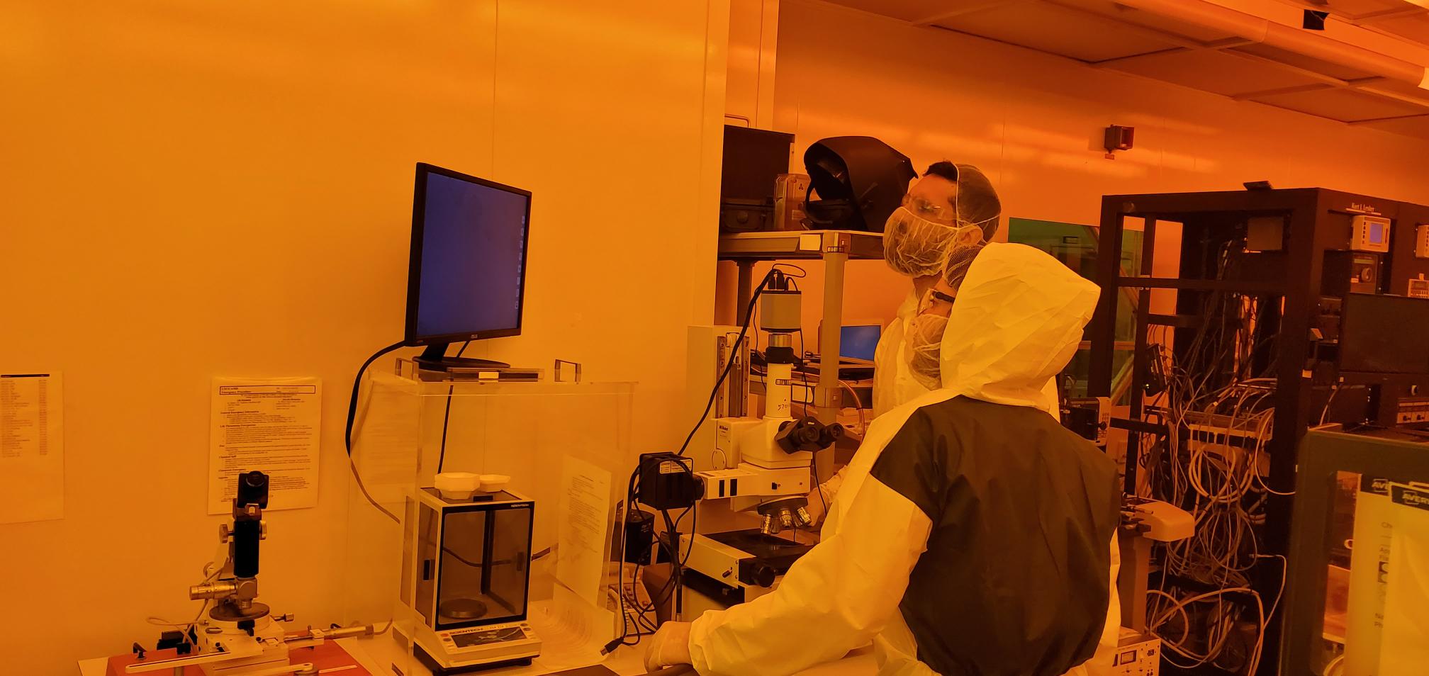
image 4 - Microscopic Inspection
Week 7 - " Second Layer Prep "
In this weeks' class students applied a layer of PMGI to their sample surface followed by resist spin coating and processing of the second layer. Students verified the process by microscopic review and SEM imaging.
.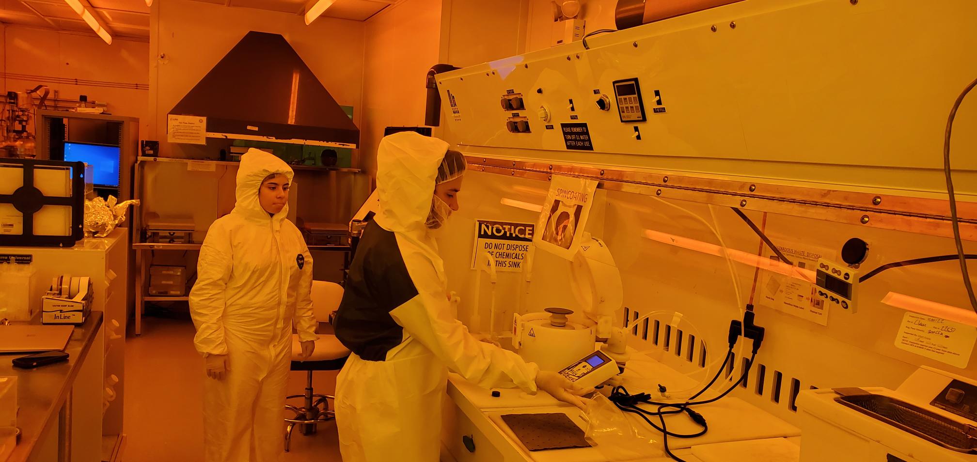
image 1 - PMGI layer
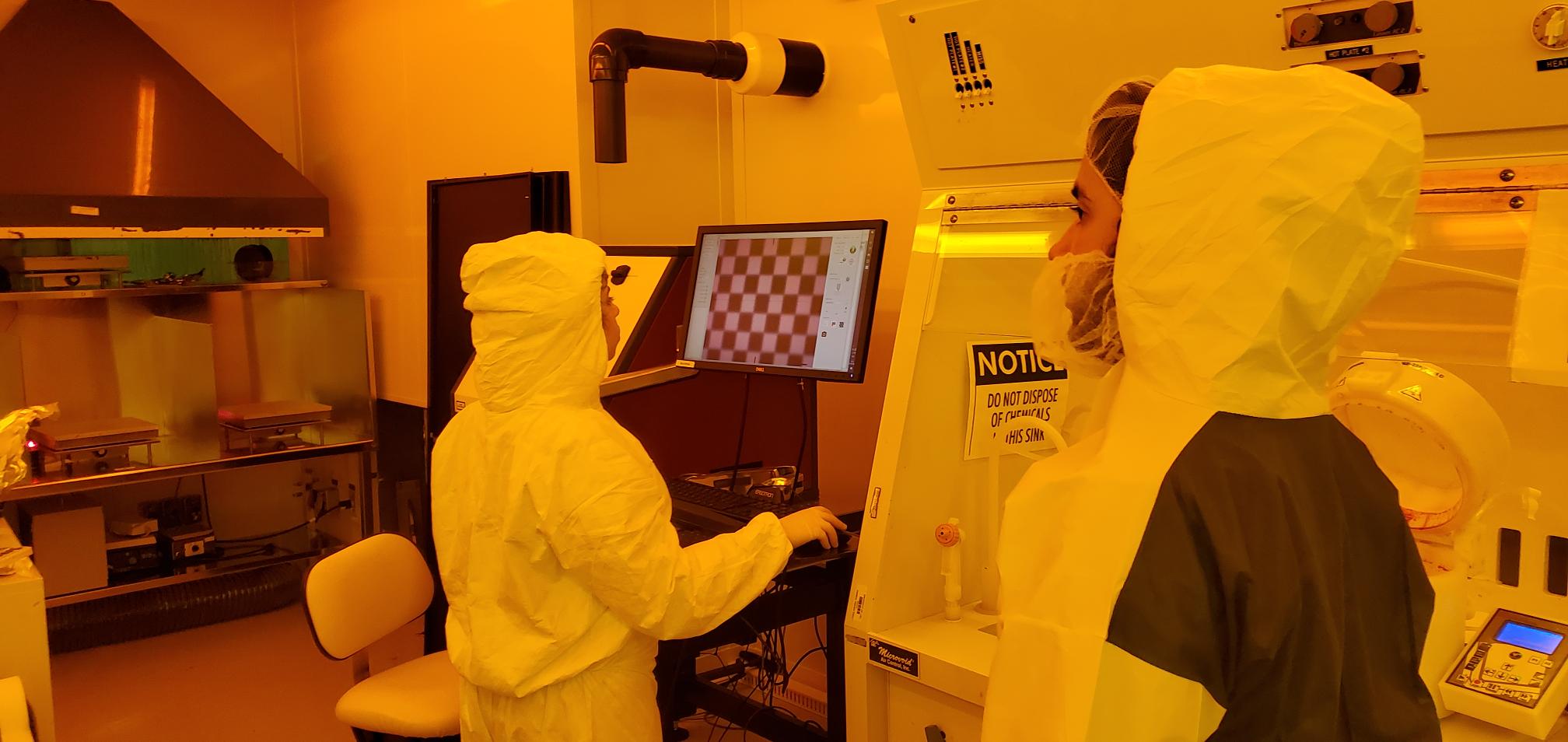
image 2 - Second Layer Exposure
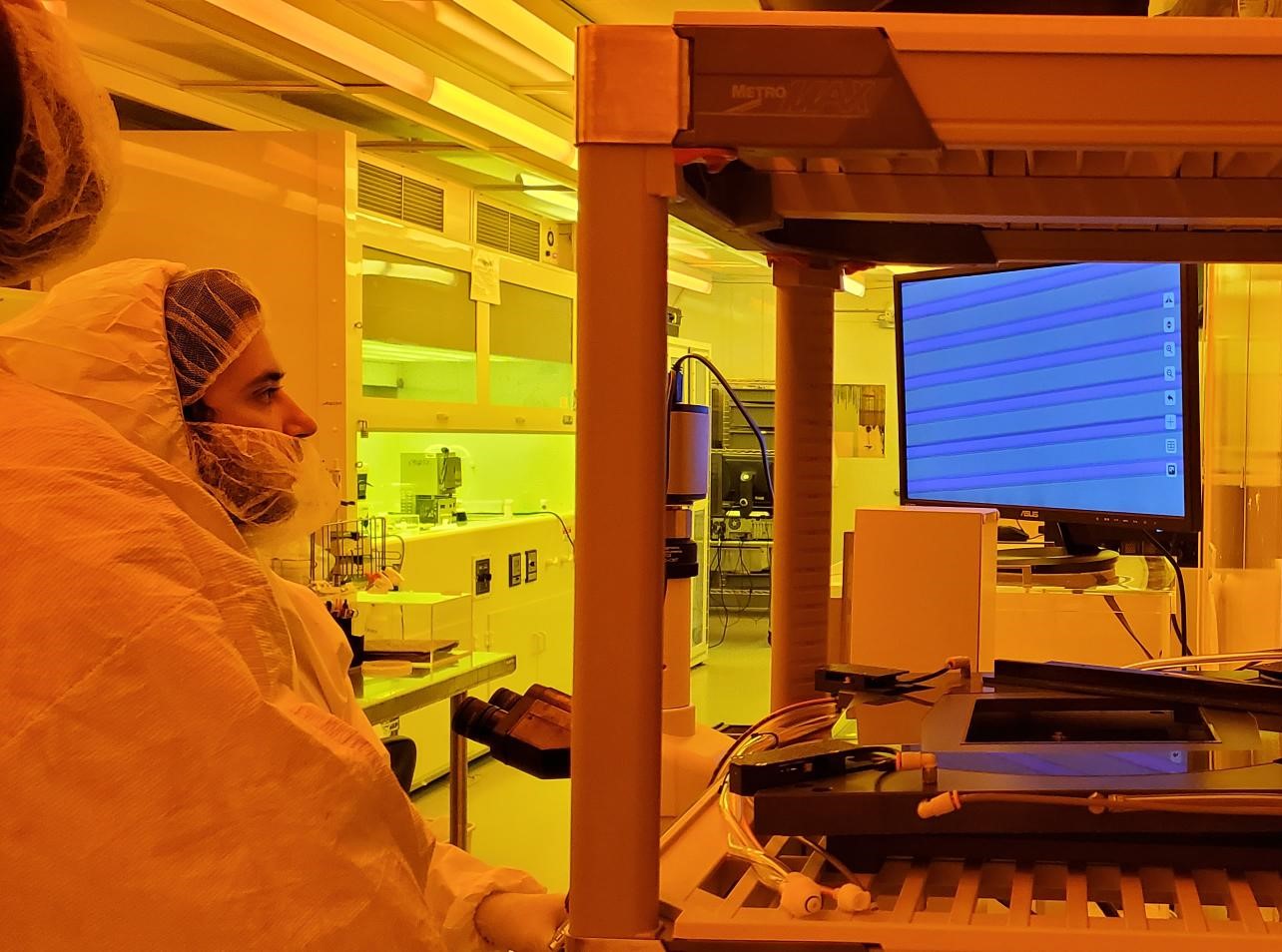
image 3 - Microscopic Inspection
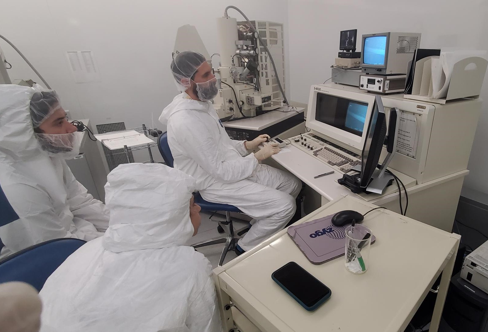
image 4 - SEM Imaging
Week 8 - "Atomic Force Microscopy"
Students learned the basic principles of how to use an AFM. The class began with students learning how to change tips and load samples properly followed by software review and class discussions.
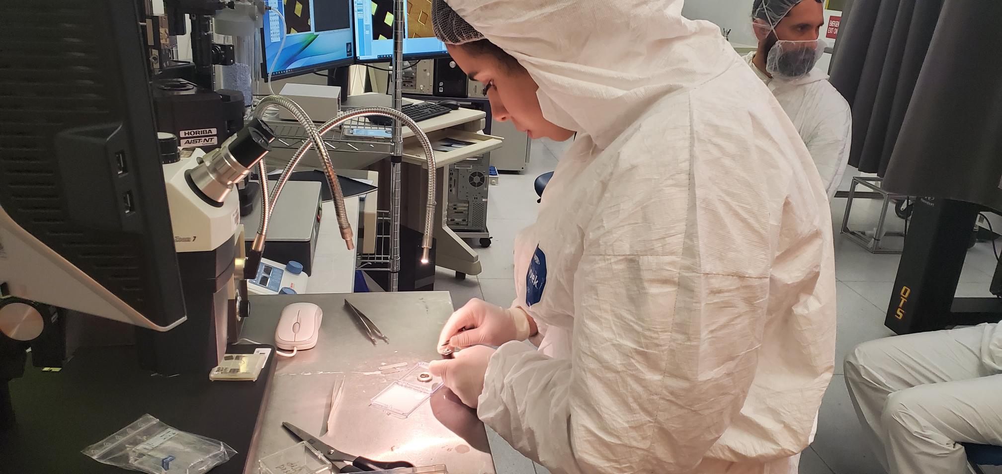
image 1 - Tip Change
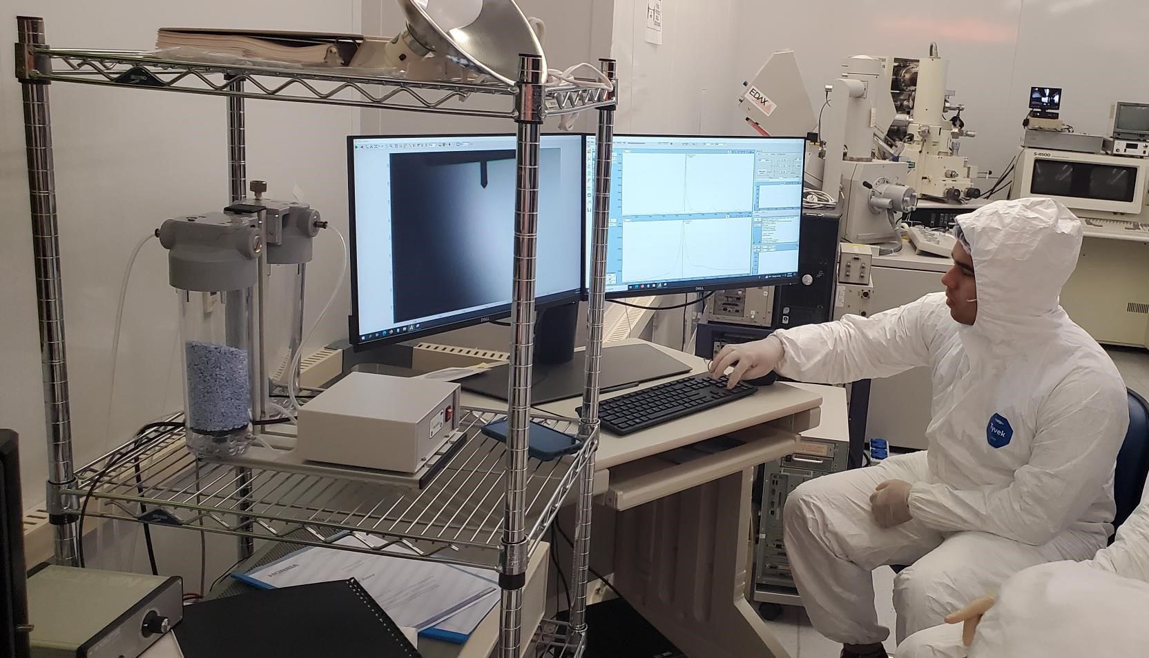
image 3 - Practice Scans
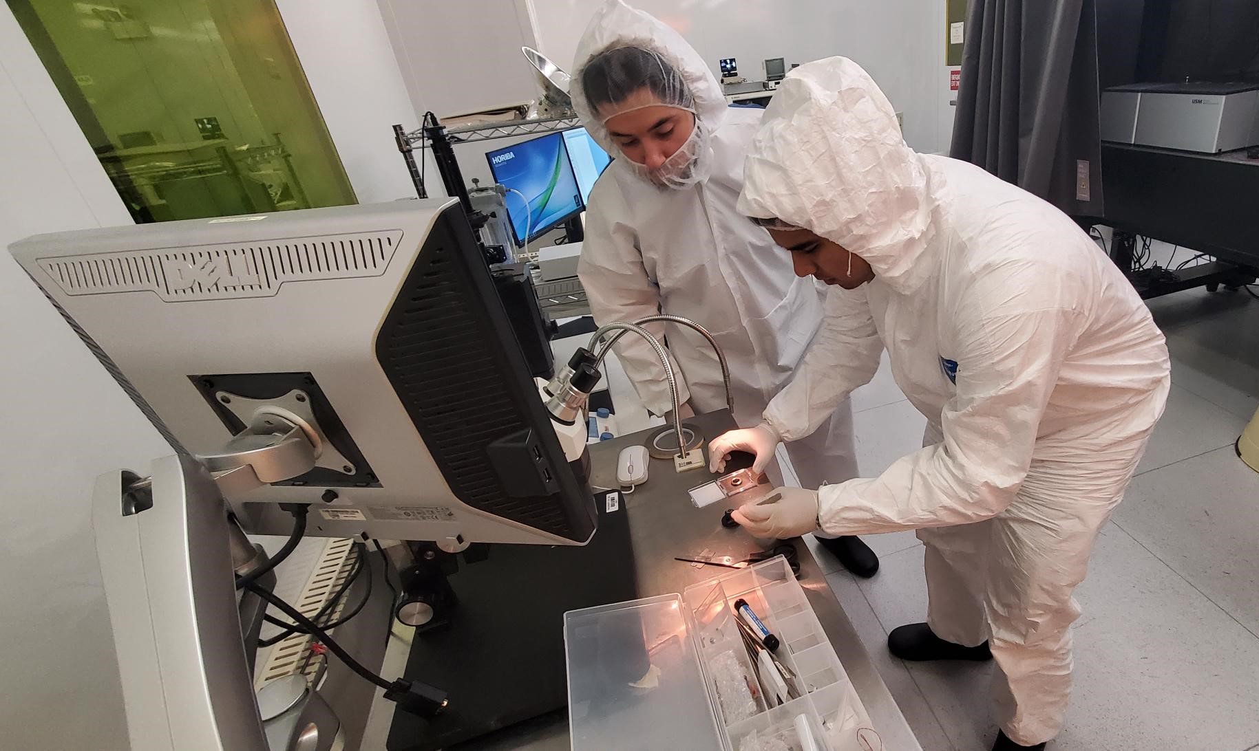 image 2 - Sample Load.
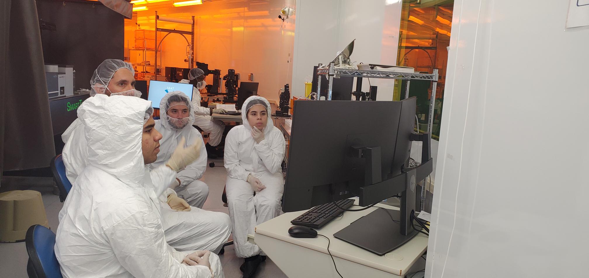
image 4 - Data Discussion
Week 9 - "Third Layer Prep"
This week students' applied the third layer to their samples leading to the final stages of the device fabrication process.
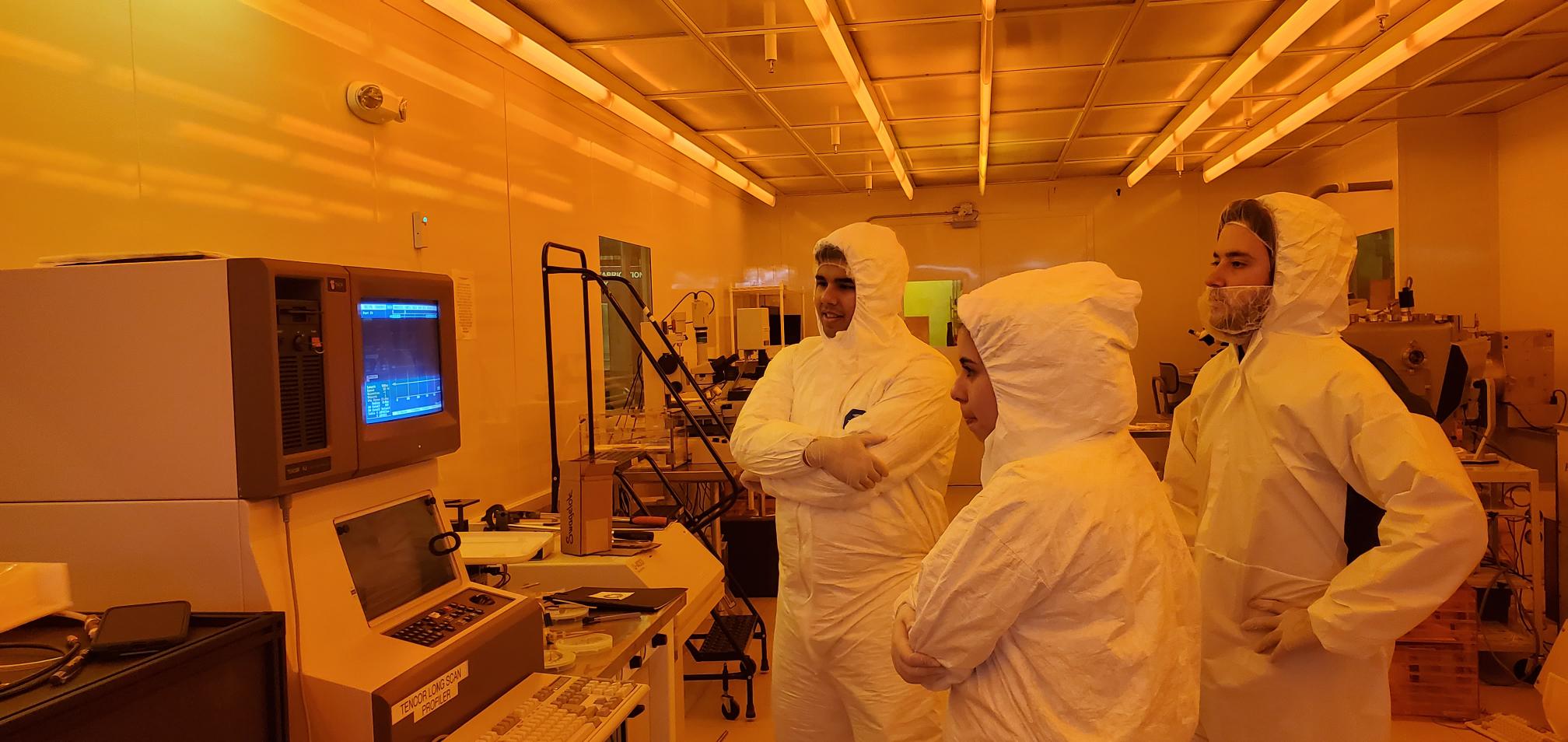
image 1 - Step height and roughness measurements
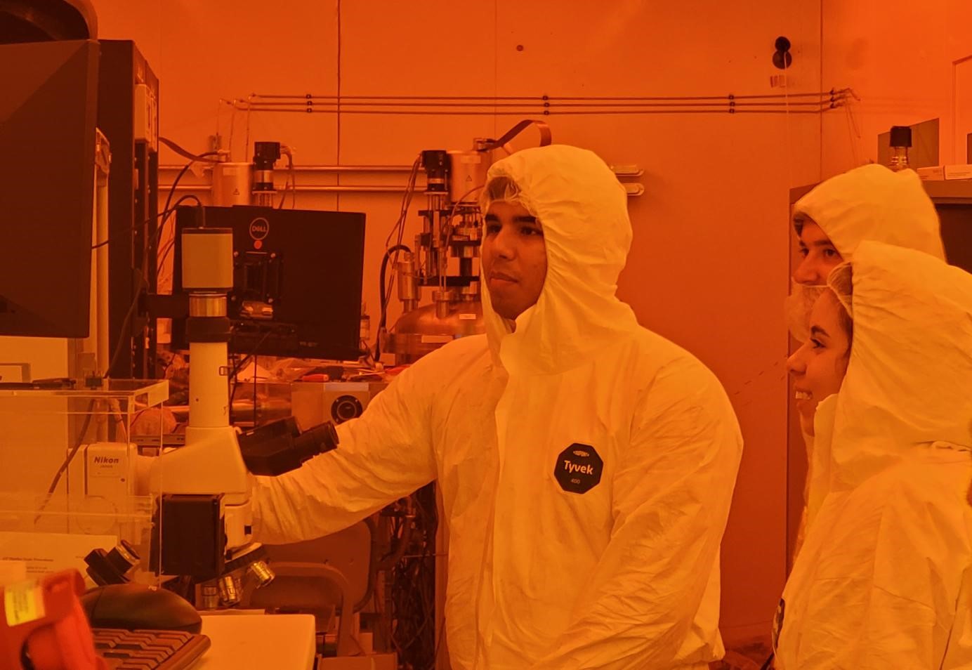
image 3 - Microscopic Review
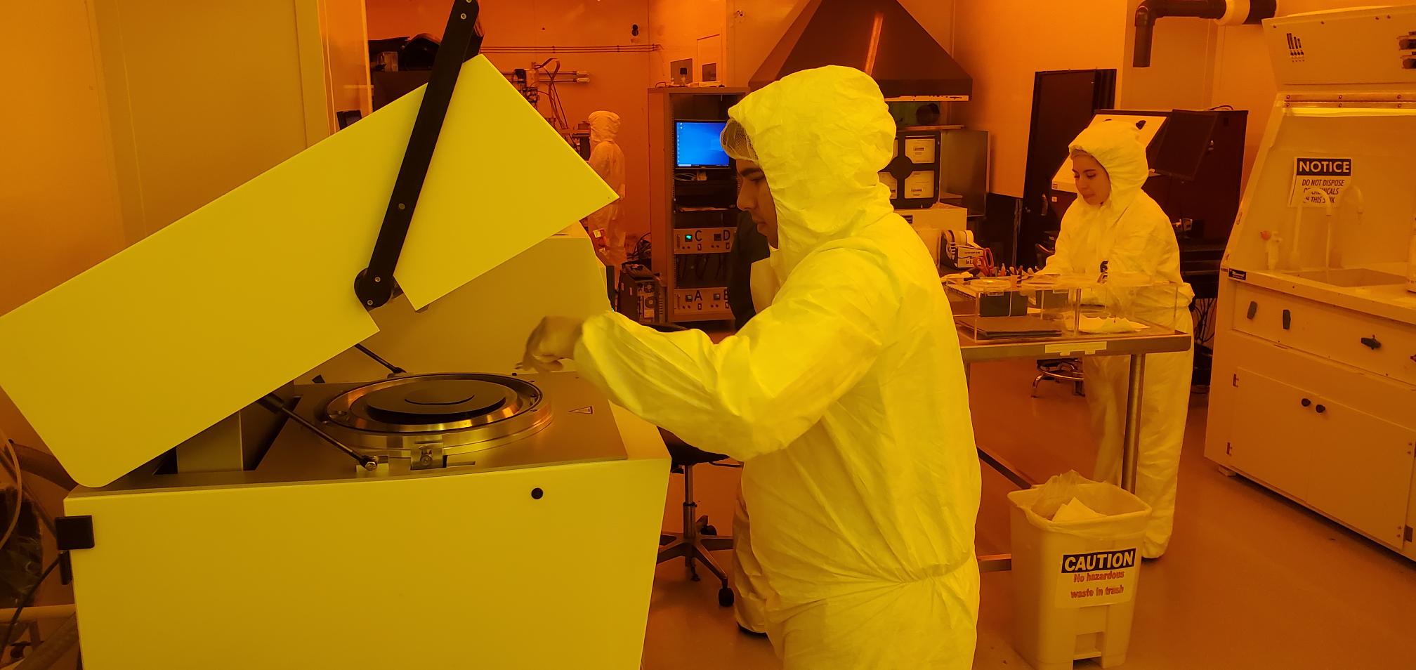
image 2 - (RTA) Rapid Thermal Annealing
.image 4 - Third layer application
Week 10 - " Preparing the final Layer"
This week the final layer of the student's samples were exposed and developed. Students were trained to use the updated software for the Oxford Plasma source used to remove remaining organic residue. Students were also introduced to the basics of Ebeam Evaporation in preparation for metal layer deposition during next week's class.
image 1 - Oxford Software Review
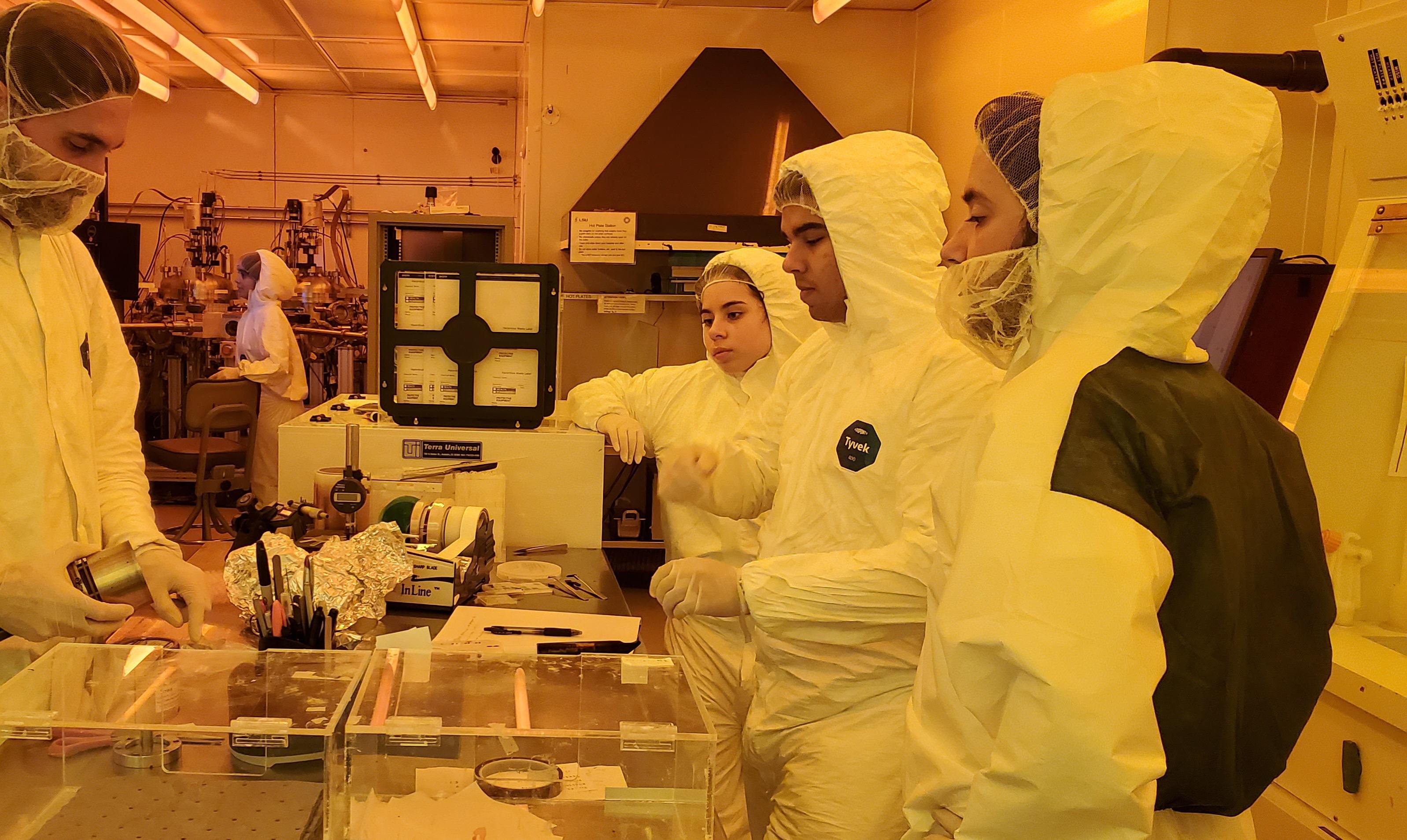
image 3 - Intro to Metal Deposition
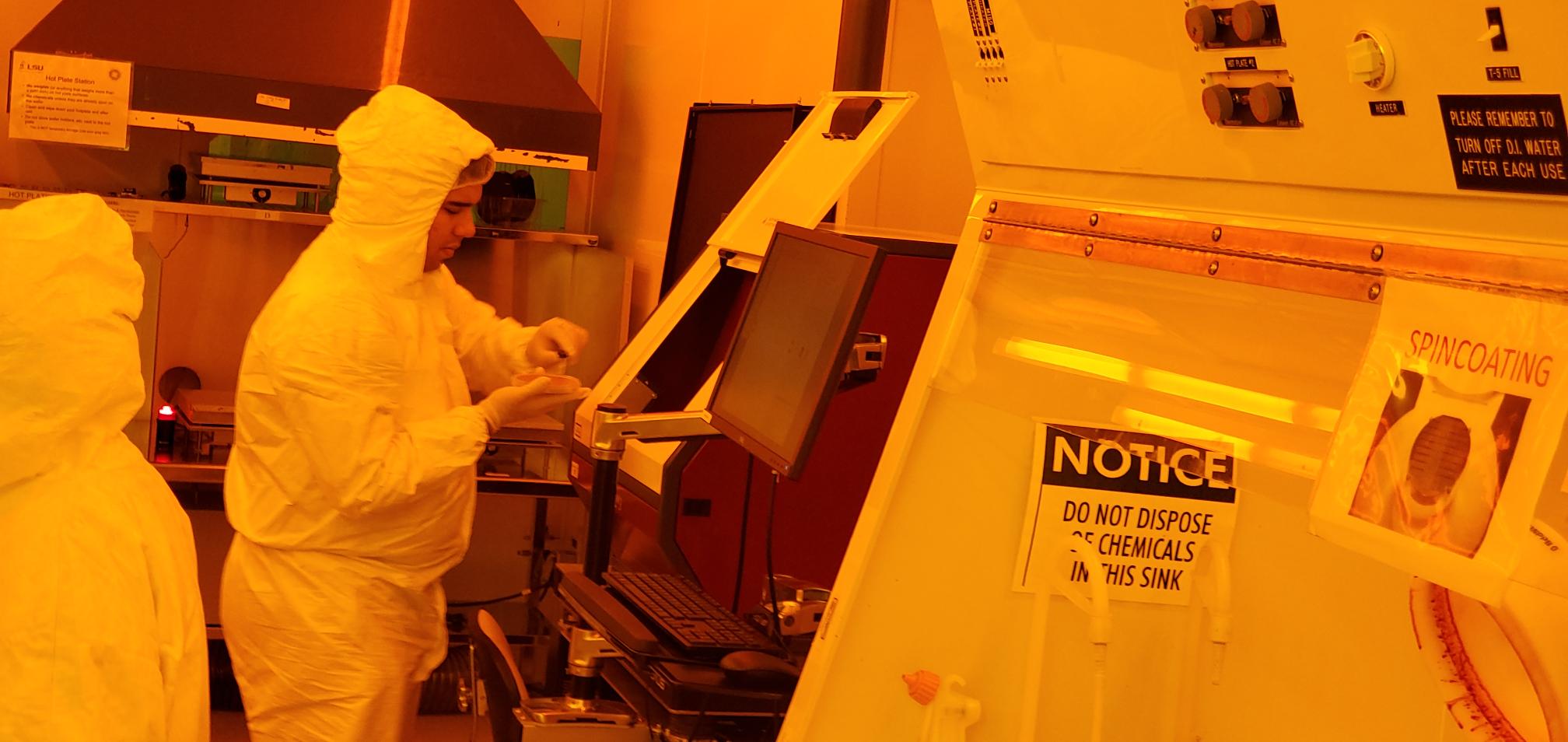
image 4 - 3rd Layer Exposure
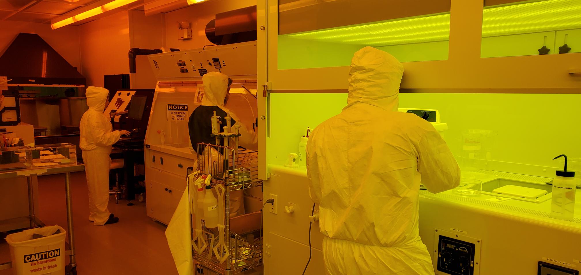
image 2 - Developing, Stripping & Cleaning
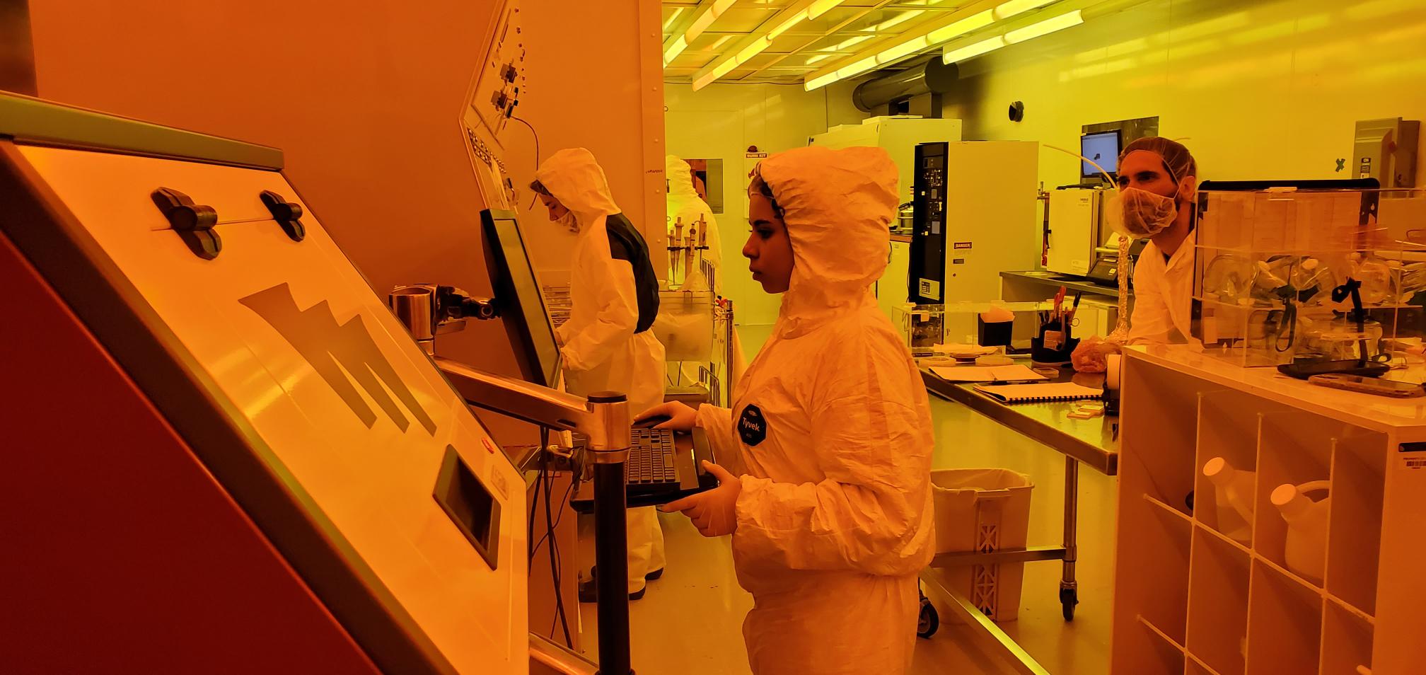
image 5 - Preview of Exposed Layer
Week 11 - " Preparing the Final Layer II"
Student's verified all three layers were properly exposed. Then deposited a metal layer by E-Beam Evaporation followed by the "lift-off" process with Acetone to remove the metal layer and remaining photoresist. Lastly students reviewed their samples by SEM imaging.
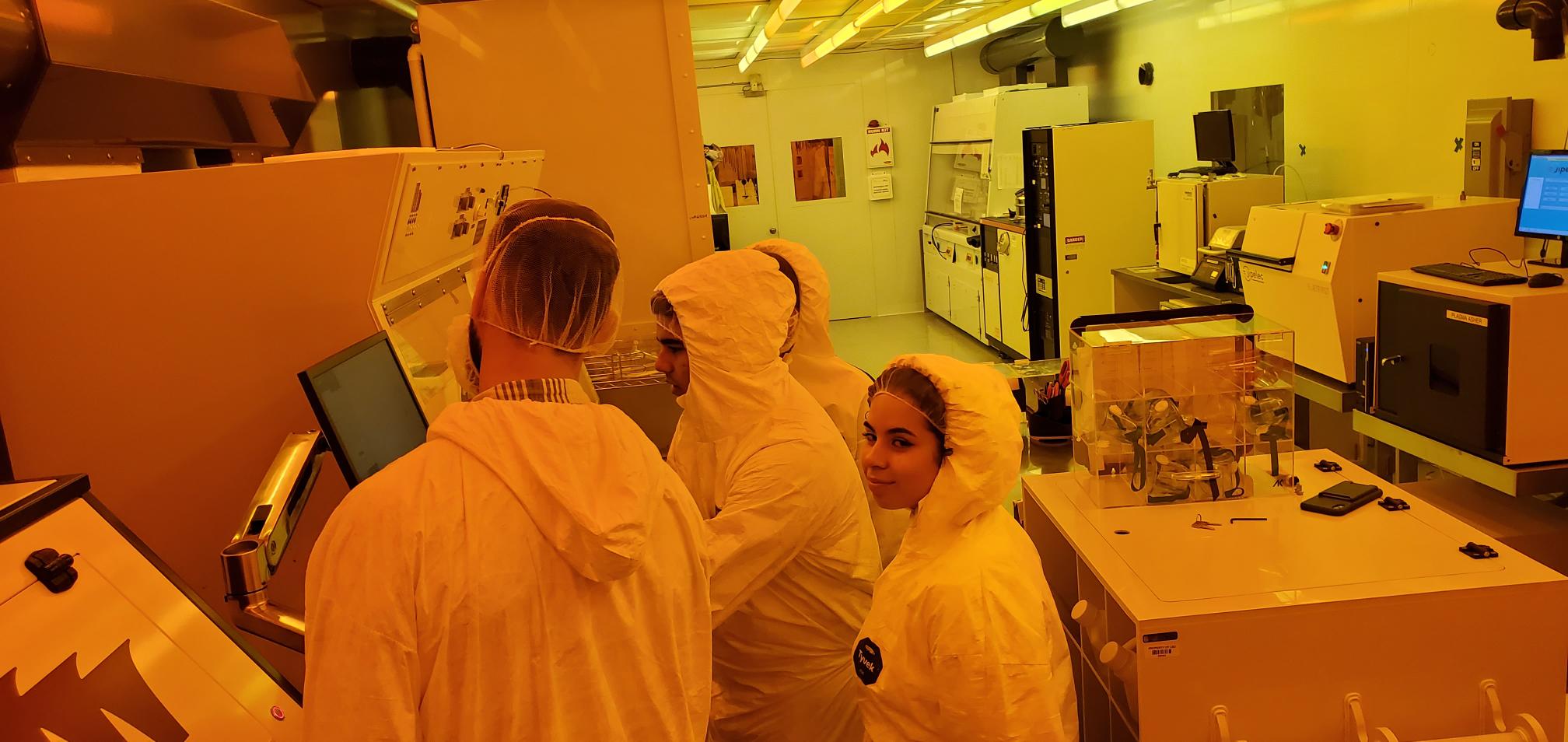
image 1 - Final Review of Exposed Layers
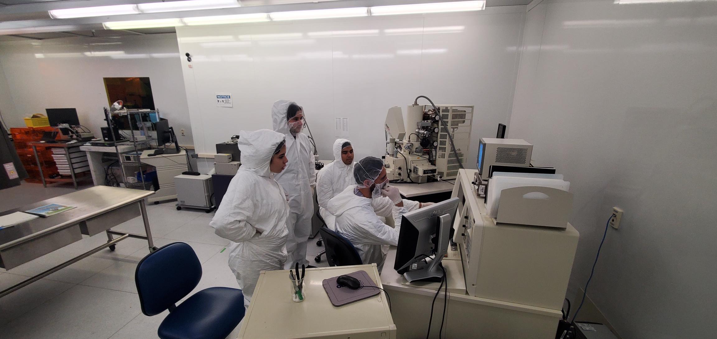
image 3 - (SEM)
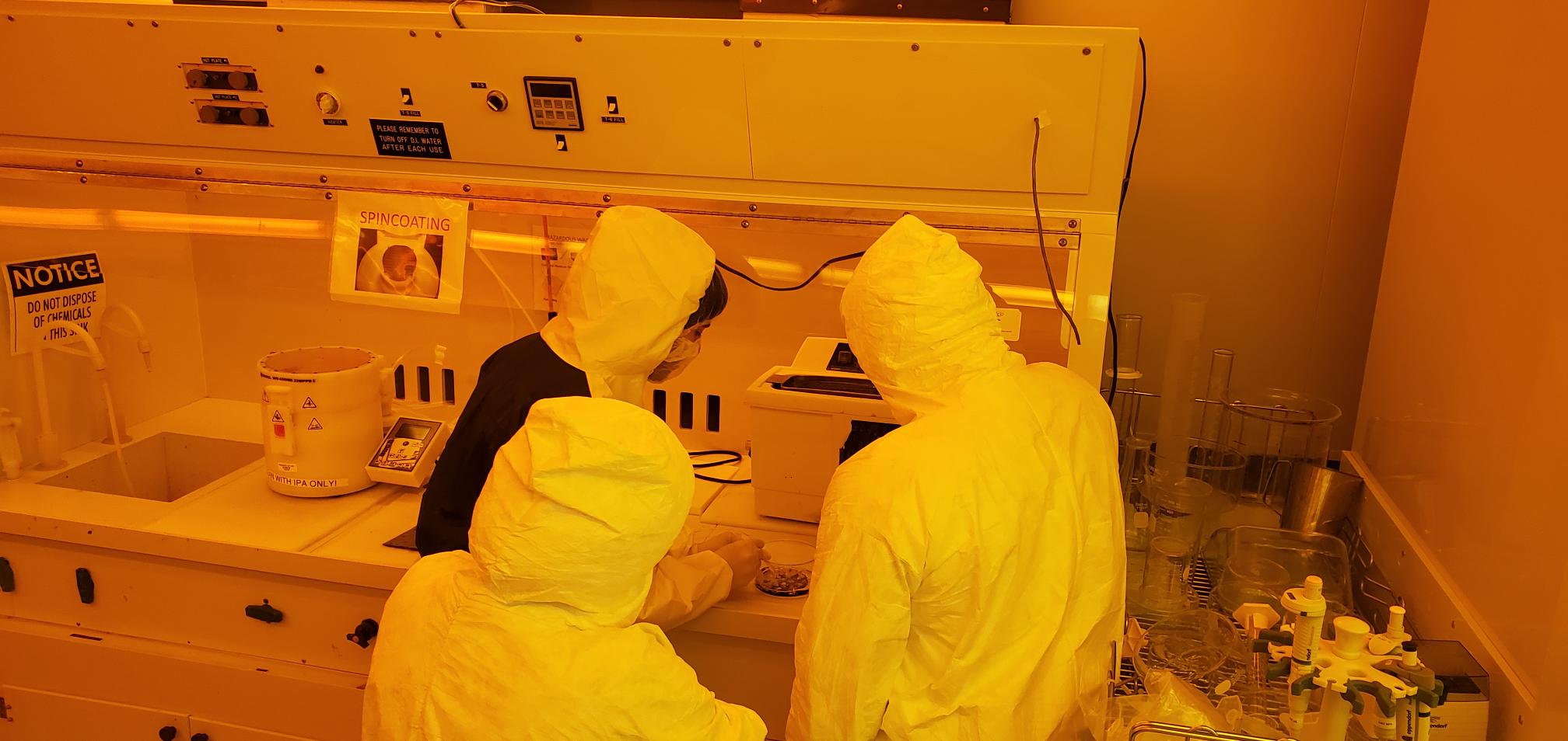
image - 3 Metal Layer "Lift-Off"
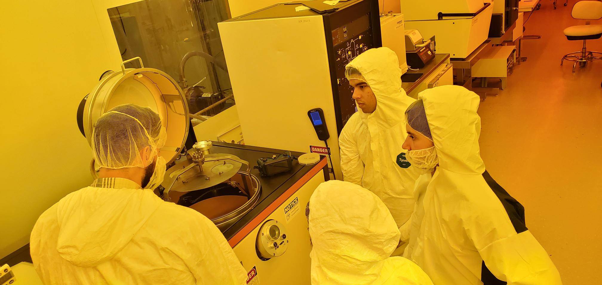
image 4 - Ebeam Evaporation
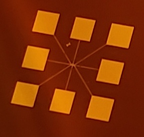
Week 12 - "The Device"
The last class concluded with students identifying signals from the newly fabricated device with use of the Mechanical Probe Station.